
Annealing has been found to be an effective means of tailoring the height of a Schottky barrier between gold and gallium nitride. This finding offers promise for the development of improved metal contacts on GaN semiconductors. Heretofore, the commercialization of GaN semiconductor devices has been impeded by difficulties of fabrication and by nonreproducibility of the Schottky-barrier heights and other properties of the metal/GaN interfaces. Now it appears that annealing may be the key to making GaN devices with smaller unit-tounit variations of contact properties and, in particular, tailorability of Schottky-barrier heights over a wide energy range.
Prior attempts to tailor Schottky contact properties had focused on details of surface cleaning and of growth and bulk properties of GaN. These attempts were not successful: unit-to-unit variations were still observed, even after cleaning and growth under controlled conditions. Although the causes of these variations are still not fully understood, more recent studies led to a partial explanation and to the annealing approach: It appears that the growth of GaN can result in a near-surface region wherein there are nonequilibrium concentrations of vacancies in Ga and N sites. These concentrations depend on aspects of the growth process that are difficult to control. These vacant sites act, variously, as electron acceptors or donors within the GaN semiconductor. As such, these sites affect the Schottky contact properties.
It was hypothesized that annealing of GaN prior to deposition of metal could be beneficial for tailoring Schottky contact properties because by suitable choice of annealing conditions (time, temperature, and either nitrogen atmosphere or high vacuum), it should be possible to produce a surface region with (1) a desired composition somewhere within a range from Ga-rich to N-rich and (2) corresponding values of near surface doping and Schottky-barrier height. This hypothesis was investigated in experiments on GaN specimens that were cleaned with HCl, then annealed prior to deposition of Au by vacuum evaporation. The specimens were then probed by ballistic-electron-emission microscopy (BEEM) for measurement of interface transmission efficiencies and Schottky-barrier heights. For comparison, some specimens were subjected to cleaning by HCl but not annealed. Other specimens were cleaned by other chemical treatments; these specimens were also not annealed. In the absence of annealing, neither the HCl treatment nor the other chemical treatments yielded substantial increases in interface transmission.
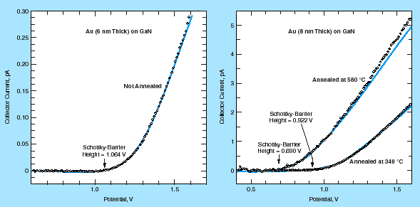
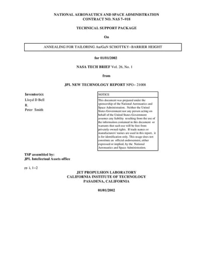
The figure shows a typical BEEM spectrum for a specimen that was not annealed, and for two other specimens that were annealed in ultrahigh vacuum for 15 minutes — one at a temperature of 340 °C and one at a temperature of 580 °C. Features of BEEM spectra can be correlated with interface properties. The voltage threshold for the onset of measurable current yields the interface Schottky-barrier height, and the magnitude of the current above this threshold indicates the fraction of the electrons injected by BEEM can cross the interface. This in turn gives information on the ideality of the interface, i.e., interface quality. Changes in these interface properties result in changes in features of the BEEM spectra. The figure shows that Schottky-barrier heights decrease, and interface transmission increases, as annealing temperature is increased. Other spectra taken after annealing at other temperatures confirm this trend. It has also been determined from BEEM spectroscopy that the starting interface properties and the direction of their change with temperature depend partly on the previous thermal history of the specimen. The changes in Schottky-barrier heights have been interpreted in terms of the creation of vacancies or the diffusion of vacancies toward the GaN surface.
This work was done by L. Douglas Bell and R. Peter Smith of Caltech for NASA’s Jet Propulsion Laboratory. For further information, access the Technical Support Package (TSP) free on-line at www.nasatech.com/tsp under the Materials category.
NPO-21008
This Brief includes a Technical Support Package (TSP).
Annealing for Tailoring Au/GaN Schottky-Barrier Height
(reference NPO-21008) is currently available for download from the TSP library.
Don't have an account?
Overview
The document is a NASA Technical Support Package detailing research on the annealing process for tailoring the Schottky barrier height between gold (Au) and gallium nitride (GaN) semiconductors. The work, conducted by a team including Lloyd D. Bell and R. Peter Smith, addresses significant challenges in the commercialization of GaN devices, which have been hindered by fabrication difficulties and nonreproducibility of Schottky barrier heights.
The Schottky barrier height is a critical parameter influencing the performance of devices such as photodetectors and high-frequency amplifiers. Historically, achieving control over this barrier height has been problematic, as it has not been fully manageable through growth conditions or surface cleaning procedures. Variations in interface properties during device fabrication have led to inconsistent performance.
The document outlines a novel approach where annealing GaN at moderate temperatures prior to metal deposition can significantly and reproducibly affect the Schottky barrier height. This method was demonstrated to alter the properties of metal contacts on GaN in a controllable manner by adjusting the annealing conditions. The research indicates that the near-surface region of GaN can contain excess gallium or nitrogen vacancies, which act as acceptors and donors, respectively. These vacancies complicate the control of interface properties during growth, necessitating a reliable method for achieving reproducible characteristics.
The findings suggest that annealing can mitigate the issues associated with low Schottky barrier heights, which have been observed even when lower bulk defect densities are achieved. By employing this annealing technique, the researchers aim to enhance the reliability and performance of GaN-based devices, making them more viable for commercial applications.
The document emphasizes the importance of reproducible interface properties for practical device fabrication and highlights the potential of annealing as a key process in achieving this goal. Overall, the research represents a significant advancement in the field of semiconductor technology, particularly for GaN devices, which are critical for various high-performance applications in electronics and optoelectronics.