Lead and its compounds have been widely used for many years in the electronics industry. However, the global demand to reduce the use of hazardous materials has compelled electronics manufacturers to consider the use of lead-free materials in future products. This transition has heightened the necessity for new finite element material models that can be used to evaluate the reliability of lead-free solders.
Lead solders, such as the popular tinlead variety, have been used in the electronics industry for the past 50 years. Subsequently, their long-term reliability is well understood. However, lead and its compounds are highly toxic and the entry of these materials into the environment has become an issue of great importance. In conjunction with legislation requiring the eventual use of leadfree materials, the electronics industry is working towards reducing the amount of lead in end-user equipment. This transition requires the development of new analytical capabilities for estimating the reliability of components that use lead-free solder.

The Ball-Grid-Array (BGA) model used in this application was built using an ABAQUS/CAE custom application of ABAQUS Version 6.6 finite element analysis developed at Worley Parsons PTE Limited, Singapore. Scripting and GUI toolkit interfaces of ABAQUS software allowed the development of certain classes of models to be automated.
The process of building a BGA model is captured in several icons such as the Model icon, the Material icon, and the Load icon. For example, only the dimensions for a BGA model need to be specified in the Model dialog box, and the model is built and meshed automatically.
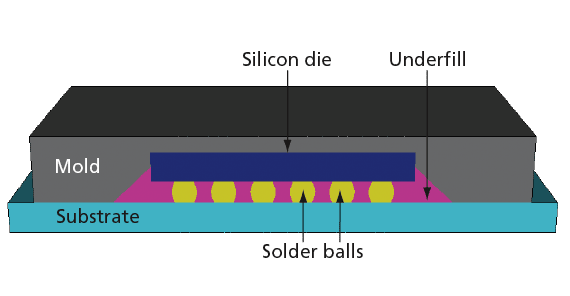
Figure 1 shows a section of the BGA model used in the present calculations. Thirty-six solder balls connect the silicon die and the substrate, with underfill material used in the space surrounding the solder balls. All components except the substrate are encapsulated in the mold.
The materials have different thermal expansion coefficients, causing stresses to develop when the model is subject to thermal loading. For simplicity, it is assumed that the entire model is subject to uniform thermal cycling. In a more detailed analysis, the temperature field could be obtained from a previous heattransfer analysis, or the entire simulation could be carried out as a fullycoupled temperaturedisplacement analysis. The bottom of the substrate is fixed and no other direct mechanical loading is applied.


The fast-growing application of lead-free materials in the electronics industry has brought new challenges with regards to the simulation of creep behavior. The advanced features of ABAQUS /Standard, including a large material library, extensive nonlinear analysis capability, and thermalmechanical coupling, have made it a powerful design tool for the electronics industry in the lead-free era.
This work was done by SIMULIA, Providence, RI. For more information, click here .

