
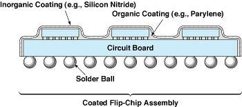
A method for protective packaging of multichip modules and related assemblies of microelectronic circuitry involves coating the assemblies with composite organic/inorganic layers only 1 to 2 mils (0.025 to 0.05 mm) thick. The method is suitable for a variety of advanced packages of microelectronic circuitry, including "chip-on-flex" circuitry, "smart" cards, flip-chips, flip-flips (flip-chips assembled onto ball-grid-array substrates), and such three-dimensional assemblies as stacked memory arrays.
Older methods for protective packaging of electronic circuitry include the following:
- Conventional hermetic sealing in metal or ceramic. This method provides effective protection. However, conventional hermetic enclosures add considerable weight and are relatively bulky [0.15 to 0.25 in. (4 to 6 mm) deep]; thus, conventional hermetic sealing defeats advances in miniaturization.
- Encapsulation in epoxy. Epoxy encapsulants can be applied to depths about one-fourth of those of conventional hermetic packages, but even at these depths, they add unacceptable amounts of weight and bulk. Epoxies are too rigid for use on the new generation of flexible multichip modules. Epoxies are also susceptible to penetration by moisture; in other words, they do not necessarily protect the packaged circuitry against moisture.
- Vapor deposition of a thin film of parylene (a thermoplastic polymer made from para-xylene). Such a film is susceptible to penetration by moisture and to thermal oxidation at temperatures greater than approximately 120 °C.
In the present method, one coats the assembled circuitry with a thin film of parylene, followed by a thin film of silicon oxide or silicon nitride (see figure). Both the organic (parylene) and inorganic (silicon-based) films are deposited at relatively low temperatures (between 25 and 100 °C). The outer inorganic film acts as a barrier to moisture and protects the underlying organic film against oxidation at temperatures up to 200 °C or even somewhat higher. The thin composite organic/inorganic film thus affords almost as much protection as does heavier, bulkier conventional hermetic packaging. The cost of depositing the composite organic/inorganic film is a small fraction of the cost of conventional hermetic packaging.
Although two-layer coats of the type described above are viable, the inorganic outer layers can be broken by mechanical handling. Therefore, it can be desirable to deposit a third (intermediate) layer for protection against mechanical stress (the third layer also provides additional protection against oxidation). For example, one can deposit a base organic layer of Parylene C (a commercial type of parylene), followed by a second organic layer of Cyclotene [or equivalent poly(benzocyclobutene)], followed by an outer inorganic layer.
In the three-layer case described above, one must take special care to cure the second organic layer according to the manufacturer's specifications, to (1) avoid compromising the base organic layer, (2) ensure a full cure to make the second organic layer relatively invulnerable to oxidation, and (3) ensure a smooth, hard second organic layer, over which the final inorganic layer can act as an effective barrier against oxygen. The basic concept can be extended to four or more layers, provided that due consideration is given to adhesion and compatibility between layers. The concept can also be extended to include other materials: For example, other inorganic coating materials that have been considered but not yet evaluated include silicon carbide, silicon oxynitride, and zirconium oxide.
This work was done by Frederick Pool and James Licari of Caltech for NASA's Jet Propulsion Laboratory. NPO-20304
This Brief includes a Technical Support Package (TSP).
Organic/inorganic coats for packaging of microelectronics
(reference NPO20304) is currently available for download from the TSP library.
Don't have an account?
Overview
The document discusses innovative protective packaging methods for microelectronics, particularly focusing on multichip modules and advanced electronic assemblies. Traditional packaging techniques, such as hermetic sealing in metal or ceramic, are effective but bulky and heavy, which contradicts the trend towards miniaturization in electronics. These conventional methods can add significant weight and volume, making them unsuitable for modern applications.
The new approach involves the use of composite organic/inorganic coatings that are only 1 to 2 mils (0.025 to 0.05 mm) thick. This method provides excellent conformal coverage, moisture impermeability, and stability at temperatures exceeding 200 °C. The primary materials used in this packaging technology include Parylene, a thermoplastic polymer, and silicon-based inorganic films. The Parylene layer serves as a base, while the inorganic layer acts as a barrier against moisture and oxidation, significantly enhancing the protection of the underlying circuitry.
Additionally, the document introduces a trilayer concept that incorporates a third layer of Cyclotene (benzocyclobutene) to provide mechanical protection and further oxidative resistance. This multilayer approach ensures that the packaging can withstand mechanical handling and environmental stresses, which is crucial for applications in high-reliability sectors such as aerospace, military, and medical electronics.
The document emphasizes the cost-effectiveness of this new packaging technology, which is a fraction of the cost of traditional hermetic packaging. It highlights the suitability of this method for various advanced electronic applications, including chip-on-flex circuits, smart cards, and three-dimensional stacked memory arrays.
Overall, the document presents a significant advancement in microelectronic packaging, addressing the need for low-cost, non-hermetic, yet highly reliable solutions that align with the demands of modern electronics. This innovative approach not only enhances the performance and durability of electronic devices but also supports the ongoing trend of miniaturization, making it a valuable contribution to the field of microelectronics.