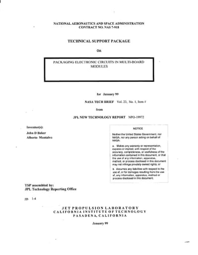
The Multi-Board Module (MBM) scheme has been conceived to provide a cost-effective way to combine digital electronic circuits into dense, lightweight packages, within which high-speed signals can be transmitted readily along three-dimensional conductive paths with minimal lengths. As the title suggests, the MBM scheme involves stacking of circuit boards in modules. Unlike in other circuit-packaging schemes, neither cables nor traditional electrical connectors are used to make the electrical connections among circuit boards in a module. Inasmuch as connectors and cables typically occupy a large fraction of the volume and constitute a large fraction of the mass of a package, the MBM scheme offers the potential for significant reductions in size and weight.

As shown in the figure, the connections between two adjacent circuit boards are made via gold-plated beryllium/copper contact springs. Each contact spring is soldered to printed wiring at a via hole on one of the boards. During assembly, each spring is pushed into contact with the printed wiring at a via hole at the corresponding location on the adjacent board. Inserts made of silicone rubber can be used to reinforce the contact springs.
In addition to eliminating the cost, weight, and bulk of cables and traditional electrical connectors, this contact scheme affords several advantages:
- The contacts are self-aligning and structurally reliable.
- Maintenance, repair, and testing are possible because circuit boards can readily be removed from stacks.
- To facilitate testing, one can turn off selected contacts by inserting insulating tabs; alternatively or in addition, one can insert thin conductive pads at selected contacts to gain access for probing.
- Unlike in conventional edge connection and in other three-dimensional-connection schemes, contacts can be located almost anywhere on the circuit boards; this makes it possible to reduce signal-path lengths and thereby accommodate higher-speed signals.
In applying the MBM concept, designers might have to contend with limits on the sizes of modules and with guidelines regarding the numbers and placements of contacts and structural supports. High circuit densities could give rise to a need for thermal straps for additional heat sinking. Under some circumstances, it could be necessary to design against a tendency for contacts to open when the circuit boards are subjected to strong vibrations.
This work was done by John D. Baker and Alberto Montalvo of Caltech for NASA's Jet Propulsion Laboratory. For further information, access the Technical Support Package (TSP) free on-line at www.techbriefs.com under the category.
In accordance with Public Law 96-517, the contractor has elected to retain title to this invention. Inquiries concerning rights for its commercial use should be addressed to
Technology Reporting Office
JPL
Mail Stop 122-116
4800 Oak Grove Drive
Pasadena, CA 91109
(818) 354-2240
NPO-19972
This Brief includes a Technical Support Package (TSP).

Packaging Electronic Circuits in Multi-Board Modules.
(reference NPO19972) is currently available for download from the TSP library.
Don't have an account?
Overview
The document discusses a novel approach to packaging electronic circuits known as the Multi-Board Module (MBM) technology, developed by NASA's Jet Propulsion Laboratory. This innovative scheme aims to create dense, lightweight packages for digital electronic circuits, facilitating the transmission of high-speed signals through three-dimensional conductive paths with minimal lengths.
One of the key features of the MBM technology is its elimination of traditional cables and connectors, which typically occupy significant volume and mass in electronic packages. By stacking circuit boards within modules and using gold-plated beryllium-copper contact springs for electrical connections, the MBM design allows for a more compact assembly. This connectorless approach not only reduces the overall size and weight of the modules but also enhances circuit performance by minimizing signal path lengths, thereby increasing circuit speed.
The document outlines the fabrication process for the contact elements used in the MBM, which involves bending and tempering beryllium-copper sheets to create the necessary contact shapes. The installation of these contacts is performed manually, but future production runs are expected to utilize precision stamping and bending techniques for efficiency.
Applications for the MBM technology are highlighted, particularly in radar systems and aerospace, where high-speed electronics are required in limited volumes. The potential for developing low-volume modules with generic functionality that can be easily integrated into spacecraft, aircraft, or scientific instruments is emphasized. The document also notes possible disadvantages, such as size limitations, the need for additional thermal management, and potential environmental challenges related to vibration during operation.
In summary, the MBM technology represents a significant advancement in electronic circuit packaging, offering a cost-effective solution that condenses existing packaging techniques while improving performance. The document concludes with a call for further development, including the construction of working prototypes and testing for electrical performance, thermal management, and vibration resilience. This innovative approach could pave the way for more efficient and effective electronic systems in various high-tech applications.

