
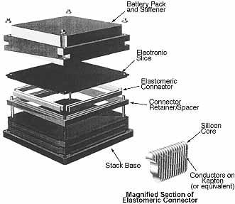
The term "space cube" denotes a scheme for three-dimensional stacking and interconnection of electronic-circuit modules. [This scheme should not be confused with a related one described in "Stackable Electronic Computer Modules and Interconnections" (NPO-19521), NASA Tech Briefs, Vol. 20., No. 6 (June 1996), page 33.] The figure illustrates a typical first-generation "space cube" stack. Each module in the stack is called a "circuit slice." The circuit slices are squares with edges 3.5 in. (8.89 cm) long, and with 160 electrical contacts on each edge. Electrical connections between corresponding contacts on adjacent modules are made by use of conductive strips on square elastomeric rings that are held in square retainer/spacer frames.
There is no particular limit on the thickness of a slice, on the material(s) of which it can be made, or the circuitry it can contain. For example, a circuit slice could be a multichip module; that is, it could contain multiple integrated-circuit chips on a printed-wiring board.
This work was done by Gary Bolotin and John Cardone of Caltech for NASA's Jet Propulsion Laboratory.
In accordance with Public Law 96-517, the contractor has elected to retain title to this invention. Inquiries concerning rights for its commercial use should be addressed to
Technology Reporting Office
JPL
Mail Stop 122-116
4800 Oak Grove Drive
Pasadena, CA 91109
(818) 354-2240
Refer to NPO-20236
This Brief includes a Technical Support Package (TSP).
First-generation "space cube" electronic-circuit packaging
(reference NPO20236) is currently available for download from the TSP library.
Don't have an account?
Overview
The document discusses the "First-Generation Space Cube" electronic-circuit packaging, a novel technology developed by Gary S. Bolotin and John M. Cardone at NASA's Jet Propulsion Laboratory (JPL). This innovative scheme focuses on the three-dimensional stacking and interconnection of electronic circuit modules, referred to as "circuit slices." Each circuit slice measures 3.5 inches (8.89 cm) on each side and features 160 electrical contacts along each edge, allowing for efficient electrical connections between adjacent modules.
The Space Cube design utilizes elastomeric connectors and conductive strips on square elastomeric rings, which facilitate the interconnection of circuit slices without the need for traditional interboard wiring or a backplane. This results in a high packaging density and symmetrical interconnections on all four edges of each module, making it a versatile solution for various electronic applications. The slices can be made from different materials and are not limited in thickness, allowing for the integration of multiple integrated circuit chips on a single printed wiring board, potentially functioning as multichip modules (MCMs).
The document highlights the advantages of the Space Cube technology, including its modularity, which enables the development of a 3D interconnect system that can be tailored for specific applications. For instance, one of the connectors can be designated as a PCI bus, while others can be allocated for different functions such as camera interfaces, MicroLan, and solar array input power. The flexibility in assigning connectors allows for customization based on the needs of the electronic system.
The work is part of NASA's ongoing efforts to advance electronic packaging technologies, and the document serves as a technical disclosure of the invention. It emphasizes the potential for commercial use and provides contact information for inquiries regarding rights to the technology.
Overall, the Space Cube represents a significant advancement in electronic circuit packaging, offering a compact, efficient, and flexible solution for modern electronic systems, particularly in aerospace and other high-tech industries. The document serves as a technical report detailing the invention's novelty, technical specifications, and potential applications.