
Integrated circuits have been invented for managing the charging and discharging of such advanced miniature energy-storage devices as planar arrays of microscopic energy- storage elements [typically, microscopic electrochemical cells (microbatteries) or microcapacitors]. The architecture of these circuits enables implementation of the following energy- management options:
- Dynamic configuration of the elements of an array into a series or parallel combination of banks (subarrays), each array comprising a series or parallel combination of elements;
- Direct addressing of individual banks for charging and/or discharging; and
- Disconnection of defective elements and corresponding reconfiguration of the rest of the array to utilize the remaining functional elements to obtain the desired voltage and current performance.
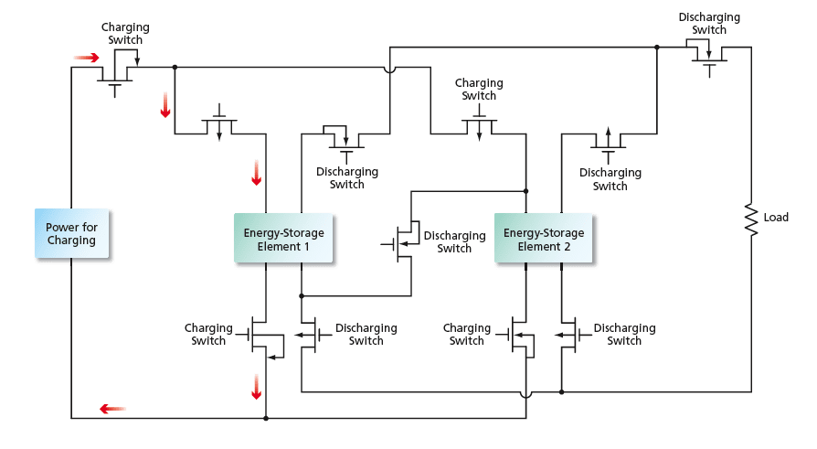
An integrated circuit according to the invention consists partly of a planar array of field-effect transistors that function as switches for routing electric power among the energy-storage elements, the power source, and the load (see figure). To connect the energy-storage elements to the power source for charging, a specific subset of switches is closed; to connect the energy- storage elements to the load for discharging, a different specific set of switches is closed.
Also included in the integrated circuit, but omitted from the figure for the sake of simplicity, is circuitry for monitoring and controlling charging and discharging. The control and monitoring circuitry, the switching transistors, and interconnecting metal lines are laid out on the integrated-circuit chip in a pattern that registers with the array of energy-storage elements. There is a design option to either (1) fabricate the energy-storage elements in the corresponding locations on, and as an integral part of, this integrated circuit; or (2) following a flip-chip approach, fabricate the array of energy-storage elements on a separate integrated-circuit chip and then align and bond the two chips together.
This work was done by Mohammad Mojarradi, Mahmoud Alahmad, Vinesh Sukumar, Fadi Zghoul, Kevin Buck, Herbert Hess, Harry Li, and David Cox of Caltech for NASA's Jet Propulsion Laboratory.
In accordance with Public Law 96-517, the contractor has elected to retain title to this invention. Inquiries concerning rights for its commercial use should be addressed to:
Innovative Technology Assets Management
JPL
Mail Stop 202-233
4800 Oak Grove Drive
Pasadena, CA 91109-8099
(818) 354-2240
E-mail:
Refer to NPO-43318, volume and number of this NASA Tech Briefs issue, and the page number.
This Brief includes a Technical Support Package (TSP).
Electronic Switch Arrays for Managing Microbattery Arrays
(reference NPO-43318) is currently available for download from the TSP library.
Don't have an account?
Overview
The document discusses an innovative solution developed by NASA's Jet Propulsion Laboratory (JPL) for managing microbattery arrays, specifically addressing the challenges posed by defective battery elements within these arrays. Micro batteries are often arranged in an array format to minimize defects, but faulty elements can act as loads, diminishing the overall capacity of the battery bank. The invention aims to screen out these defective elements and configure the remaining micro batteries into optimal series or parallel combinations to achieve desired voltage and current performance for various loads.
The proposed solution involves a solid-state circuit architecture that facilitates the interrogation, programming, and charging of the micro batteries with specific characteristics tailored to maximize their lifespan. Central to this architecture is an array of solid-state switches that serve as routing and multiplexing tools connected to the batteries. These switches allow for the selective connection of batteries for charging and discharging, enhancing the efficiency of the battery management system.
The document highlights the integration of the solid-state switches with charging and charge monitoring circuitry on the same chip, which can be connected to the battery array using flip-chip technology or through direct deposition of the batteries onto the chip. This miniaturized approach is particularly suited for the highly compact energy storage elements developed under the NASA NRA program, with potential applications extending to other energy storage systems, such as capacitor arrays.
The novelty of this invention lies in its ability to dynamically configure micro batteries into series or parallel combinations and to directly address individual banks of batteries for charging. This flexibility is crucial for optimizing the performance of micro batteries in various applications, particularly in aerospace and other high-tech fields.
Overall, the document serves as a technical support package under NASA's Commercial Technology Program, aiming to disseminate aerospace-related developments with broader technological, scientific, or commercial implications. For further inquiries or assistance, the document provides contact information for JPL's Innovative Technology Assets Management.