
Two closely related methods of optical inspection and computation yield data on misalignments between critical features in different layers of microfabricated devices. Examples of such devices containing features in different layers that are required to be aligned with each other include (1) magnetic-memory devices containing magnetic and nonmagnetic metal lines and grooves in garnet substrates, (2) integrated electronic circuits containing variously patterned metal, semiconductor, and dielectric materials, and (3) micromechanical devices. Before the development of the present methods, misalignments were determined in manual/visual procedures, in which technicians took readings from vernier or wedge test structures.
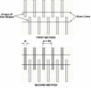
The present methods also involve the use of test structures, but most of the work of taking the readings and processing the data is automated. The test structures comprise arrays of parallel stripes of width w and pitch p = 4w (see figure). These arrays are fabricated as integral parts of the layers to be inspected. Nominally, in a given test structure, the arrays in two layers of interest are parallel to each other, with the long axes of the stripes perpendicular to the coordinate axis along which misalignment is to be measured (hereafter called "the axis of interest," for short).
During inspection, a video camera is focused on the device through a high-power microscope to capture an image of the arrays of stripes. The image is digitized, and the resulting data are processed on a personal computer. The processing includes three major tasks, the first of which is a "line scan," in which digitized image intensities are taken as functions of position (with a resolution of 1 pixel) along two lines that are nominally parallel to the axis of interest. The second major task is to compute correlations between the line scans. The third major task is to determine the misalignment distance from the locations of the peaks of the correlation function.
The practices described thus far in general terms are common to both methods. The methods differ in the locations of test structures and line scans and in the associated details of computing the misalignments from the line-scan data. In the first method, the test structures are placed near each other (but not overlapping), and separate line scans are taken through the two structures. This method is valid only when deviation of the scan line from orthogonality to the test stripes is so small that any apparent shift caused by this deviation is a small fraction of a pixel.
The second method is more complex but offers the advantage of eliminating the requirement of orthogonality. In this method, the two test structures are partly interdigitated, and two line scans are performed. The first line scan is taken through whichever test structure is more clearly defined in the video image. The second line scan is taken through both test structures in the overlap region. In this method, the shift associated with nonorthogonality and the misalignment between the test structures are computed from a combination of the correlation between both line scans of the first test structure and the correlation between the line scans of the two structures. In an experiment, these methods yielded data on misalignments between grooves in a garnet substrate and metal stripes (in another layer) with an error less than half of the 0.5-µm fabrication tolerance of the specimen.
This work was done by Udo Lieneweg of Caltech for NASA's Jet Propulsion Laboratory. For further information, access the Technical Support Package (TSP) free on-line at www.techbriefs.com under the Manufacturing/Fabrication category, or circle no. 106 on the TSP Order Card in this issue to receive a copy by mail ($5 charge). NPO-20016
This Brief includes a Technical Support Package (TSP).
Extracting Misalignments of Layers in Microfabricated Devices.
(reference NPO20016) is currently available for download from the TSP library.
Don't have an account?
Overview
The document presents a technical support package from NASA detailing innovative methods for extracting misalignments in microfabricated devices, specifically focusing on microelectronic and micromechanical structures. The primary challenge addressed is the precise alignment required between different layers of materials, such as conductive and nonconductive elements, which is crucial for the functionality of devices like magnetic-memory chips and integrated circuits.
Historically, alignment verification relied on manual methods using vernier or wedge-type test structures, which were prone to human error and limited by poor contrast in shallow grooves. The new approach leverages automated optical inspection techniques to enhance accuracy and efficiency. The proposed methods utilize arrays of parallel stripes, designed with a specific width and pitch, integrated into the layers of interest. These arrays are positioned either close to each other or in an interdigitated manner to facilitate alignment measurement.
During the inspection process, a high-power microscope captures images of the stripe arrays, which are then digitized and processed using a personal computer. The analysis involves three major tasks: performing a line scan to obtain intensity data from the images, computing correlations between the line scans of different layers, and determining the misalignment distance based on the correlation function's peak locations.
The document outlines two methods for extracting misalignment data. The first method correlates intensity sequences from scans of two parallel layers, while the second method focuses on interdigitated regions. By analyzing the maxima in the correlation function, the relative positions of the stripes in the two layers can be calculated, providing a precise measurement of misalignment.
This automated optical extraction procedure significantly improves the reliability of alignment measurements in microfabrication, addressing the limitations of previous manual techniques. The document emphasizes the importance of accurate alignment in the performance of microelectronic and micromechanical devices, particularly in applications involving micromagnetic structures on garnet substrates, where traditional electrical methods are not viable due to the nonconductive nature of the material.
Overall, the document highlights a significant advancement in the field of microfabrication, showcasing how automation and optical techniques can enhance the precision of alignment measurements, ultimately contributing to the development of more reliable and efficient microfabricated devices.