
A rectangular integrated-circuit focal-plane array of 640 × 486 GaAs/AlxGa1 -xAs quantum-well infrared photodetectors (QWIPs) constitutes the image sensor in an experimental long-wavelength infrared camera. This is the first long-wavelength infrared camera containing photodetectors in a focal-plane array that enables imaging in a format similar to that of standard television. The camera, which is sensitive to wavelengths between 8 and 9 µm, can be operated in a staring, snapshot, or video mode.
Until now, state-of-the-art long-wavelength infrared photodetectors have been made from HgCdTe. Difficulties associated with the HgCdTe material system - especially, nonuniformity of devices in arrays - have prevented the fabrication of HgCdTe photodetectors in 640 × 486 arrays with sufficient pixel-to-pixel uniformity to obtain images of acceptable quality in the 8-to-12-µm region of the infrared spectrum. The development of the present camera was guided by the conjecture that by using large-band-gap materials like GaAs and AlxGa1 - xAs, which can be grown and processed easily, one should be able to fabricate large, relatively uniform arrays of QWIPs to detect light at wavelengths between 6 and 25 µ.

The QWIPs in the present camera are of the bound-to-quasi-bound type, for which the thermionic component of dark current is less than for other types. [This topic was discussed in more detail in "Bound-to-Quasi-Bound Quantum-Well Infrared Photodetectors" (NPO-19633), NASA Tech Briefs, Vol. 22, No. 9 (September 1998), page 54. The basic multiple-quantum-well (MQW) structure of the QWIP array is a stack of 50 identical quantum-well bilayers. Each bilayer comprises (1) a 45-Å-thick well layer of GaAs n-doped at a density ≈ 5× 1017 cm -3 and (2) a 500-Å-thick barrier layer of Al0.3Ga0.7As. The MQW structure is sandwiched between 0.5-µm-thick top and bottom contact layers of GaAs doped similarly to the well layers.
All of the aforementioned layers were grown on a semi-insulating GaAs substrate by molecular-beam epitaxy. A 300-Å-thick Al0.3Ga0.7As stop-etch layer was grown on top of the top contact layer for use in fabricating a cross-grating structure to couple light into the array. [The cross-grating-coupler concept was described in "Cross-Grating Coupling for Focal-Plane Arrays of QWIPs" (NPO-19657), NASA Tech Briefs, Vol. 22, No. 1 (January 1998), page 6a.] A 0.7-µm-thick GaAs cap layer was grown on top of the stop-etch layer. The cross-grating structure was fabricated by photolithography and dry chemical etching.
The array of 640 × 486 photodetectors, with a pitch of 25 µm and a pixel size of 18 × 18 µm2, was then formed by wet chemical etching through the MQW layers into the bottom contact layer. The cross gratings on the tops of the detectors thus formed were covered with Au/Ge and Au for ohmic contact and reflection (reflection at the top surface increases photoresponse, inasmuch as the device is operated in a back-illuminated configuration - that is, with illumination through the substrate). Indium bumps were evaporated onto the (Au/Ge)/Au layers, then the bumps were used to bond (hybridize) the array to a silicon-based complementary metal oxide/semiconductor (CMOS) integrated-circuit 640 × 486 readout multiplexer. The QWIP-array/readout-circuit hybrid was then mounted along with an antireflection-coated, 100-mm-focal-length germanium lens to form the camera (see Figure 1).
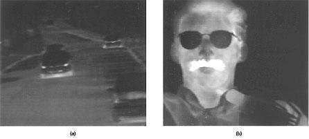
In tests, the camera produced excellent images that demonstrated high sensitivity (see Figure 2). The performance of the QWIP operating in a photoconductive (as distinguished from photovoltaic) mode at a reverse bias of 2 V, temperature of 70 K, and background temperature of 300 K was characterized by, among other things, a noise-equivalent differential temperature of 36 mK. The uncorrected nonuniformity (which includes a 1-percent nonuniformity of the readout circuit and a 1.4-percent nonuniformity of a cold stop in front of the array) was found to be only 5.6 percent.
This work was done by Sarath Gunapala, Sumith Bandara, John Liu, and Winn Hong of Caltech for NASA's Jet Propulsion Laboratory.
In accordance with Public Law 96-517, the contractor has elected to retain title to this invention. Inquiries concerning rights for its commercial use should be addressed to
Technology Reporting Office
JPL
Mail Stop 122-116
4800 Oak Grove Drive
Pasadena, CA 91109
(818) 354-2240
Refer to NPO-20312
This Brief includes a Technical Support Package (TSP).

A 640 x 486 long-wavelength infared camera
(reference NPO20312) is currently available for download from the TSP library.
Don't have an account?
Overview
The document is a NASA Technical Support Package detailing the development of a long-wavelength infrared camera that utilizes GaAs/AlxGa1-xAs quantum-well infrared photodetectors (QWIPs). This innovative camera, developed by a team from the Jet Propulsion Laboratory (JPL), represents a significant advancement in infrared imaging technology, enabling high-quality imaging in a format similar to standard television.
The camera features a rectangular integrated-circuit focal-plane array with a resolution of 640x486 pixels, making it capable of capturing detailed images in the long-wavelength infrared spectrum, specifically sensitive to wavelengths between 8 and 9 micrometers. This capability allows for various operational modes, including staring, snapshot, and video modes, enhancing its versatility for different applications.
The document highlights the camera's impressive performance characteristics, including high sensitivity and low noise levels. In tests, the QWIP operated in photoconductive mode at a reverse bias of 2 V and a temperature of 70 K, achieving a noise-equivalent differential temperature of 36 mK. The uncorrected nonuniformity of the camera was found to be only 5.6%, which includes minor contributions from the readout circuit and a cold stop in front of the array.
The development of this camera addresses previous limitations associated with traditional infrared detectors, such as those made from HgCdTe materials, by providing a more uniform and efficient alternative. The work was conducted under contract with NASA, and the inventors include Sumith V. Bandara, Sarath D. Gunapala, Winn Hong, and John K. Liu.
The document also includes a notice stating that the United States Government, NASA, and associated parties do not make any warranties regarding the information contained within and do not assume liability for its use. The camera's development is positioned as a significant contribution to the field of infrared imaging, with potential applications in various scientific and industrial domains.
Overall, this technical report encapsulates the innovative strides made in infrared camera technology, showcasing the capabilities of QWIPs and their potential to revolutionize imaging in the long-wavelength infrared spectrum.