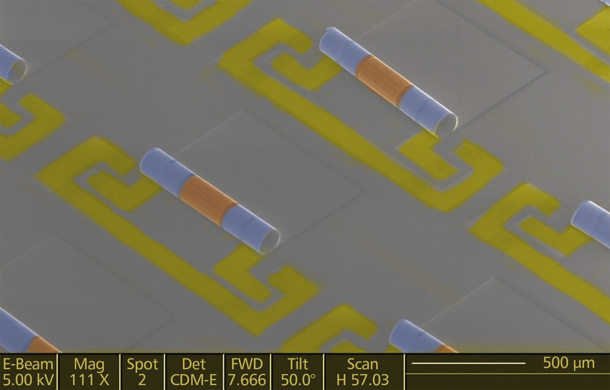
Electronic filters are part of the inner workings of phones and other wireless devices. They eliminate or enhance specific input signals to achieve the desired output signals; however, they take up space on chips. Researchers have integrated the individual elements that make up electronic filters onto a single component, significantly reducing the amount of space taken up by the device.
The conventional 2D on-chip lumped or distributed filter network design — composed of separate inductors and capacitors — was replaced by a single, space-saving, 3D rolled membrane that contains both independently designed elements. The team used a specialized etching and lithography process to pattern 2D circuitry onto very thin membranes. In the circuit, they joined the capacitors and inductors together and with ground or signal lines, all in a single plane. The multilayer membrane can then be rolled into a thin tube and placed onto a chip.
The patterns, or masks, used to form the circuitry on the 2D membrane layers can be tuned to achieve whatever kind of electrical interactions are necessary for a particular device. The team tested the performance of the rolled components and found that under the current design, the filters were suitable for applications in the 1- to 10-gigahertz frequency range. While the designs are targeted for use in radio frequency communications systems, the team believes that other frequencies, including in the megahertz range, are also possible based on their ability to achieve high power inductors in past research.
The team worked with several simple filter designs but theoretically can make any filter network combination using the same process steps.
For more information, contact Xiuling Li at


