
MEMS is a more complex technology than traditional semiconductors. They are 3D structures with moving parts, making them much more difficult to fabricate. If you’re designing a semiconductor, you may be able to take advantage of an existing process development kit (PDK), which your foundry can provide to you. There is no equivalent approach in MEMS. It’s a “one process, one product” paradigm that requires a high level of customization. That takes time, money, and resources.
The MEMS industry can’t match the rapid innovation cycles typical of the semiconductor industry — it’s been more than a decade since we’ve seen a major leap in MEMS manufacturing processes. However, I’m confident that we at Omnitron can rapidly improve the approach to manufacturing MEMS.
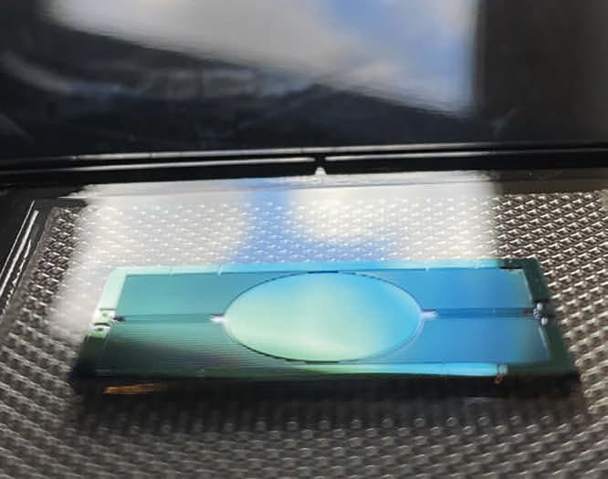
Omnitron processing combines deep reactive ion etching (DRIE), which promotes increased sensitivity and performance as well as more compact design, and silicon-on-insulator (SOI) technology, a semiconductor structure consisting of a layer of single crystalline silicon separated from the bulk substrate by a thin layer of insulator. In SOI wafers the insulator is almost invariably a thermal silicon oxide (SiO2) layer, and the substrate is a silicon wafer. By reducing parasitic capacitance, SOI boosts electrical performance — supporting lower power consumption and faster switching speeds. This improves upon the traditional surface micromachining process in which thin films are deposited and patterned on the surface of a substrate. This is a generational advancement that integrates the best of previous approaches to improve the performance, power, reliability, and cost of a wide variety of MEMS sensors, including Omnitron’s MEMS mirror.
MEMS Mirrors for LiDAR
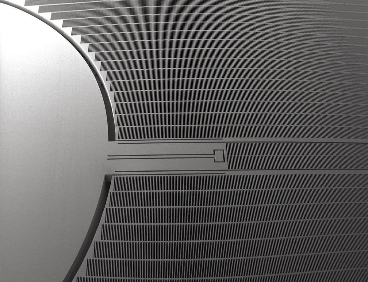
Traditional MEMS mirrors often struggle with limited range of motion and step-scanning capabilities. To overcome those challenges, Omnitron employs DRIE, followed by oxidation to create gaps and fill trenches with polysilicon. This method enables the formation of trenches up to five times deeper than those in conventional designs while maintaining very narrow gaps of 2.5 microns, extending 200 microns deep. In addition to this increased depth, Omnitron has invented a technique to leverage deep etching and polysilicon trench filling, which provides a wider range of motion, linear capacitance changes, and uniform gaps. Although these advancements are crucial for the performance and reliability of LiDAR systems in autonomous vehicles, these same advantages are useful for many other MEMS actuators as well as sensors.
Packaging
Packaging is a critical factor for MEMS devices. For example, since MEMS mirrors for LiDAR are used for automotive applications, they’re hermetically sealed to keep out dust particles.
The mirror also features a pre-tilt offset — each mirror is given a preset angular offset at the wafer level. This approach simplifies assembly and alignment for applications such as LiDAR. At the die level, it allows for simpler, lower-cost system-level assembly. Just imagine three different mirrors with three different offsets, which give you a 120-degree field of view (FOV) in an industry in which a 60-degree FOV is more common. That 120-degree FOV offers a much more accurate representation of the environment.
MEMS Mirrors for Laser Spectroscopy
Laser spectroscopy equipment can be used to monitor oil and gas pipelines for toxic gases, such as methane. As methane, like all natural elements, has its own laser-spectrum footprint, laser spectroscopy uses a mirror to scan the pipeline for the unique signature of that gas. In theory, it’s an elegant solution, but there’s a problem. The traditional scanning element used in this equipment is the galvo, a type of scanning mirror that’s expensive, fragile, and power-hungry. Galvo-based spectroscopy monitoring requires airplane flyovers to scan the environment. When we’re talking about gas leaks, intermittent monitoring isn’t good enough.

Omnitron’s MEMS mirrors, in contrast, are low-cost and rugged, and support a wide FOV and step-scanning. They’re also much lower power than a galvo because Omnitron’s scanning mirror consumes just milliwatts of power, a tiny fraction of the power consumed by galvo scanning solutions, which typically consume more than 20W. The upshot is that laser spectroscopy equipment using Omnitron’s MEMS mirror performs accurate and continuous real-time monitoring of oil and gas pipelines.
Photonics-Based MEMS Mirrors for AI Data Centers
The potential of MEMS mirrors to improve speed and power efficiency for routing optical signals in an AI datacenter is especially compelling, particularly when such datacenters consume a massive amount of power.
As AI workloads and hyperscale data centers push the limits of traditional networking, optical circuit switching (OCS) is emerging as a critical solution to overcome bandwidth bottlenecks, reduce energy consumption, and enhance scalability.
Omnitron is pioneering a new type of MEMS-based OCS technology that delivers faster switching speeds, lower latency, and higher switch counts — key factors in enabling the future of high-performance computing and AI-driven infrastructure. Built on the company’s high figure of merit (FoM) MEMS mirror design, Omnitron’s architecture eliminates input/output (I/O) limitations and increases tilt angles, supporting higher port counts, larger arrays, and more agile optical networks. Beyond performance, Omnitron’s simplified manufacturing process reduces the number of fabrication steps to just a handful, lowering defect densities, improving reliability, and driving down costs. In this way, the company’s foundational IP — its new topology for MEMS — enhances scalability while accelerating OCS deployment timelines for next-generation data centers.
The Bright Future for MEMS
Through Moore’s Law, we’ve been able to predict the pace of innovation in semiconductors for decades. While we can’t apply the same rubric to MEMS, startups like Omnitron Sensors are aiming to set a rate of advancement that will drive the commercialization of more affordable, resilient MEMS devices for the mass market.
This article was written by Eric Aguilar, co-founder and CEO of Omnitron Sensors. For more information, go here .