
A surface-micromachining process has been devised for use in fabricating microscopic polycrystalline diamond structures (e.g., bridges and cantilevers) as integral parts of microelectromechanical systems (MEMS). The general concept of MEMS encompasses such diverse objects as simple mechanical actuators, simple mechanical sensors, or complex units containing electronic or optoelectronic circuitry integrated with mechanical sensors and/or actuators. Because diamond is highly resistant to corrosion and is transparent, the ability to form diamond structures could contribute to the development of MEMS to withstand corrosive environments. For example, diamond structures could serve as supports for corrosion-resistant electrodes in MEMS designed for biomedical applications. MEMS containing diamond films could also prove useful as automotive sensor and display devices.
An explanation of the distinction between surface and bulk micromachining is prerequisite to a description of the present diamond-surface-micromachining process. In bulk micromachining, three-dimensional features are etched into the bulk of a crystalline or noncrystalline material. In surface micromachining, features are built up, layer by layer, on a substrate of single-crystal silicon or other suitable material. The features in a given layer are defined by dry etching or selective deposition. Then the structure containing the feature is released from the substrate by wet etching (and consequent undercutting) of the substrate material.
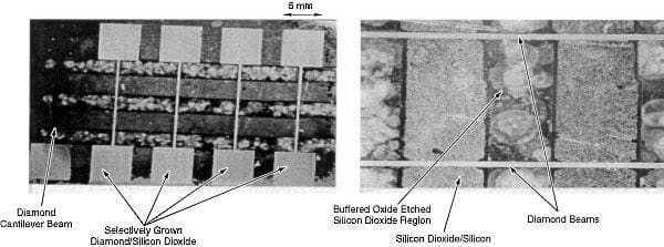
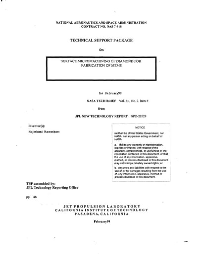
The present diamond-surface-micromachining process is best described in terms of experiments in which it was first demonstrated. The starting substrates in the experiments were mirror-smooth, (100)-oriented single-crystal silicon wafers that were, variously, p- or n-doped to a resistivity <20 ©·cm. The wafers were cleaned, then thermally oxidized to a depth of 1 to 1.5 micrometers.
Each substrate was prepared for selective deposition of diamond, following either procedure A or procedure B described below:
Procedure A. To increase the density of nucleation sites for diamond and thereby make it possible to obtain a pinhole-free diamond deposit, the surface of the oxidized substrate was damaged by ultrasonic agitation in methanol containing diamond particles. The ultrasonically damaged SiO2 substrate surface was photolithographically patterned. By use of a buffered oxide-etch solution, the wafer was partially chemically etched through the openings in the photoresist to remove the damaged oxide surface layer and thereby define the areas where diamond was not to be deposited. The photoresist was then removed by commercial stripping solutions and the substrate cleaned in an oxygen plasma.
Procedure B. The SiO2 substrate surface was photolithographically patterned, then the substrate was hard-baked at a temperature of 150 to 200°C. The substrate (with the photoresist still in place) was subjected to ultrasonic agitation in methanol containing diamond particles, so that the SiO2 surface areas exposed through the holes in the photoresist mask would be damaged and would therefore become sites for deposition of diamond. Then the photoresist was stripped off and the substrate cleaned as in procedure A.
Following procedure A or B, the substrate was cleaned, then placed in a chemical-vapor-deposition (CVD) chamber. Polycrystalline diamond was grown on the patterned and damaged SiO2 areas by CVD from a flowing mixture of methane and hydrogen, typically at a total pressure of 45 torr (6 kPa) and a substrate temperature of 950 °C.
The diamond-patterned substrate was cleaned in solvents. In a photolithographic process, a new photoresist pattern was formed to define the portions of the substrate to be etched away from the diamond. Then by use of a buffered oxide-etch solution, the SiO2 layer on the substrate was removed from under selected diamond-patterned areas, leaving diamond structures supported over airgaps (bridges and cantilevers).
This work was done by Rajeshuni Ramesham of Caltech for NASA's Jet Propulsion Laboratory.
This Brief includes a Technical Support Package (TSP).
Surface micromachining of diamond fabrication of MEMS microstructures
(reference NPO20529) is currently available for download from the TSP library.
Don't have an account?
Overview
The document is a technical support package from NASA's Jet Propulsion Laboratory (JPL) detailing research on the surface micromachining of diamond for the fabrication of microelectromechanical systems (MEMS). The focus is on the innovative techniques used to create diamond microstructures, such as bridges and cantilever beams, which are crucial for various microsensor applications.
The research highlights the advantages of using diamond in MEMS due to its unique properties, including high hardness, thermal conductivity, and chemical stability. These properties make diamond an ideal material for applications requiring durability and precision. The document discusses the fabrication processes, particularly low-pressure chemical vapor deposition (LPCVD) of polycrystalline diamond films, which allows for the creation of very flat surface micromachined features.
The document outlines the differences between surface micromachining and wet bulk micromachining, noting that while surface micromachining is limited in feature height to a few microns, wet bulk micromachining can utilize the full thickness of the wafer. It also describes the use of anisotropic chemical etching techniques to fabricate diamond microstructures, emphasizing the complexity and challenges involved in the process, such as the need for protective coatings and the careful handling of etching materials.
Additionally, the document mentions the potential applications of the fabricated diamond microstructures in various fields, including automotive safety (e.g., accelerometers for airbag deployment) and optical devices. It also discusses the patent rights status of the research, indicating that a written description has been submitted for publication and that there are no current sales or commercial applications of the technology.
The document concludes by identifying potential interest from various government agencies and companies in the innovation, suggesting a broad relevance and applicability of the research findings. Overall, this technical report serves as a comprehensive overview of the advancements in diamond microstructure fabrication and its implications for future MEMS technologies.