
A feed-horn-coupled monolithic array of micromesh bolometers is undergoing development for use in a photometric camera. The array is designed for conducting astrophysical observations in a wavelength band centered at 350 μm. The bolometers are improved versions of previously developed bolometers comprising metalized Si3N4 micromesh radiation absorbers coupled with neutron-transmutation-doped Ge thermistors. Incident radiation heats the absorbers above a base temperature, changing the electrical resistance of each thermistor. In the present array of improved bolometers (see figure), the thermistors are attached to the micromesh absorbers by indium bump bonds and are addressed by use of lithographed, vapor-deposited electrical leads. This architecture reduces the heat capacity and minimizes the thermal conductivity to 1/20 and 1/300, respectively, of earlier versions of these detectors, with consequent improvement in sensitivity and speed of response.
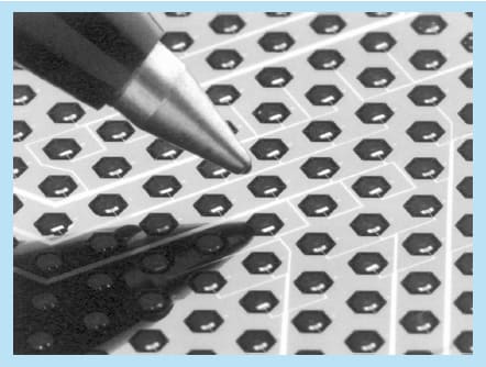
The micromesh bolometers, intended to operate under an optical background set by thermal emission from an ambient-temperature space-borne telescope, are designed such that the random arrival of photons ("photon noise") dominates the noise sources arising from the detector and readout electronics. The micromesh is designed to be a highly thermally and optically efficient absorber with a limiting response time of about 100 μs. The absorber and thermistor heat capacity are minimized in order to give rapid speed of response. Due to the minimization of the absorber volume, the dominant source of heat capacity arises from the thermistor.
The array demonstrates a dark noise-equivalent power of 2.9⋅10-17 W/(Hz)1/2 and a mean heat capacity of 1.3 pJ/K at a detector temperature of 0.390 K from a 0.300 K cold plate. The optical efficiency of the bolometer and feedhorn array, measured by comparing the responses to blackbody calibration sources, lies between 0.4 and 0.6. Photon noise dominates over detector noise arising from phonon, Johnson, and amplifier noise, as measured under the design background conditions. The ratio of total noise to photon noise is found to be 1.21 at an absorbed optical power of 2.4 pW. The array shows high stability with excess noise found to be negligible at frequencies as low as 30 mHz.
This work was done by James Bock and Anthony Turner of Caltech for NASA's Jet Propulsion Laboratory. For further information, access the Technical Support Package (TSP) free on-line at www.techbriefs.com/tsp under the Physical Sciences category.
NPO-30290
This Brief includes a Technical Support Package (TSP).
Array of Bolometers for Submillimeter-Wavelength Operation
(reference NPO-30290) is currently available for download from the TSP library.
Don't have an account?
Overview
The document is a Technical Support Package from NASA’s Jet Propulsion Laboratory (JPL) concerning the "Array of Bolometers for Submillimeter-Wavelength Operation," identified by NPO-30290. It is part of NASA Tech Briefs, which aim to disseminate aerospace-related technological advancements with broader scientific, commercial, and technological implications.
The primary focus of this document is on the innovative Spider Web Bolometer Array, which is specifically designed for sub-millimeter astrophysics. This technology is crucial for observing astronomical phenomena that emit radiation in the sub-millimeter wavelength range, which is often obscured by the Earth's atmosphere. The document references a key publication by A. D. Turner et al. from 2001, titled "Si₃N₄ Micromesh Bolometer Array for Sub-millimeter Astrophysics," published in Applied Optics, which provides further insights into the technology and its applications.
The Technical Support Package emphasizes the importance of compliance with U.S. export regulations, indicating that the information may contain proprietary data from Caltech/JPL. It also highlights the role of the Commercial Technology Program of NASA, which aims to make aerospace developments accessible for wider use beyond government applications.
For those seeking additional information or assistance regarding research and technology in this area, the document provides contact details for the Innovative Technology Assets Management at JPL, including a mailing address, telephone number, and email. This facilitates further inquiries into the technology and its potential applications.
The document concludes with a notice clarifying that the U.S. Government, nor any representatives acting on its behalf, assume liability for the use of the information contained within. It also states that any mention of trade names or manufacturers is for identification purposes only and does not imply official endorsement by NASA.
In summary, this Technical Support Package serves as a comprehensive overview of the Spider Web Bolometer Array technology, its significance in sub-millimeter astrophysics, and the broader implications of NASA's innovations in aerospace technology. It encourages collaboration and exploration of these advancements for various applications in science and industry.