
In a proposed technique for fabrication of microelectromechanical devices, thin films of fullerenes would be used as temporary packaging to protect and position delicate components. The initial application of this technique would likely occur in the fabrication of devices in which quantum-mechanical tunneling of electrons across gaps about 1 nm wide would be exploited to measure subnanometer displacements of the components facing each other across the gaps.
Typically, a tunneling device of this type includes a pyramidal metal tip that faces a gold-coated diaphragm across the tunneling gap. In present fabrication practice, the initial gap is set by moving the tip and diaphragm toward each other under manual control until a tunneling current is measured. Often, the tip and diaphragm are accidentally brought into contact, with consequent damage to either or both.
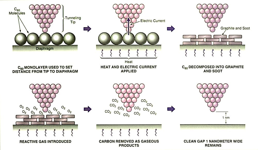
The proposed technique calls for deposition of a monomolecular layer of the fullerene C60 on the diaphragm prior to setting the gap (see figure). The C60 molecular unit is approximately spherical and, fortuitously, is 1 nm wide. Thus, the monomolecular layer of C60would not only prevent contact between the tip and diaphragm but would also automatically establish the desired gap thickness. It would still be necessary to position the tip and diaphragm as in current fabrication practice, but tunneling current would no longer be used as the position indicator; instead, exploiting the electrical conductivity of C60, one would simply monitor for contact between the tip and the C60 film, as indicated by the onset of electrical conductance between them.
Once the fullerene film had served its purpose, it would be removed (either during fabrication or at any suitable time thereafter). If the film were weakly chemisorbed on the diaphragm, it might be removable by simple heating. Otherwise, a more complex removal process would include the application of both externally generated heat and an electrical current through the tip/C60-film contact; the combination of externally supplied heat flux and current would have to be large enough to heat the C60 film in the vicinity of the tip sufficiently to break down the C60 into graphite and soot, but not so large as to damage the tip or the diaphragm. The resulting hot carbonaceous contaminants would be removed by chemical reaction with O2 (or perhaps with Cl2 and/or H2) to form CO2 and/or other gaseous species.
The O2 or other reactive gas could be supplied via a channel with a one-event valve; such channels and valves are commonly included in microelectromechanical devices and systems. The CO2 and/or other gaseous product(s) could be adsorbed onto a sacrificial (getter) surface that had been fabricated previously as an integral part of the device. As a result, the region around the tip would be free of fullerene, carbonaceous contaminants, or adsorbed gas.
This work was done by John D. Olivas of Caltech for NASA's Jet Propulsion Laboratory.
This invention is owned by NASA, and a patent application has been filed. Inquiries concerning nonexclusive or exclusive license for its commercial development should be addressed to
the Patent Counsel
NASA Management Office-JPL; (818) 354-2240
Refer to NPO-20148.
This Brief includes a Technical Support Package (TSP).
Temporary Fullerene Films in Microelectromechanical Devices
(reference NPO20148) is currently available for download from the TSP library.
Don't have an account?
Overview
The document discusses an innovative technology developed by John D. Olivas at Caltech for NASA’s Jet Propulsion Laboratory, focusing on the use of temporary fullerene films in microelectromechanical devices (MEMS). The primary goal of this invention is to enhance the reliability and quality assurance of tunneling MEMS by preventing premature contact and damage to tunneling tips during fabrication and handling.
The core of the innovation involves depositing a monolayer of C₆₀ fullerenes onto the conducting surface of a tunneling device. This protective layer maintains the precise spacing required for tunneling, which is critical for the device's functionality. The document outlines the challenges faced in the assembly of these devices, particularly the difficulty in maintaining a one-nanometer spacing between components, which is essential for their operation. Traditional methods of establishing this spacing have proven inadequate, often leading to failures due to contact between the tip and diaphragm.
Once the device reaches its intended destination, the fullerene layer can be removed through the application of thermal and/or electrical energy. This process breaks down the fullerene into carbonaceous contaminants, which are then eliminated by reacting with a specific gas (such as O₂, H₂, or Cl₂). The resulting molecular species have a greater tendency to form gases that can be desorbed from the surfaces, thus cleaning the tunneling region and ensuring optimal conditions for operation.
The document emphasizes the novelty of this approach, highlighting its potential applications beyond tunneling devices to a broader range of microelectromechanical and nanoelectromechanical systems. The use of fullerenes not only serves as a protective measure but also as a fabrication technique that ensures precise spacing, thereby improving the overall performance and reliability of these advanced technologies.
In summary, this work represents a significant advancement in the field of MEMS, addressing critical challenges in device assembly and operation through the innovative use of fullerene films. The technology is poised to enhance the functionality and durability of tunneling devices, contributing to the ongoing development of sophisticated micro and nano-scale systems.