
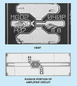
A prototype W-Band, low-noise amplifier has been fabricated by bump-bonding a high-speed, low-noise InP high-electron-mobility (HEMT) transistor onto the previously fabricated passive portion of the amplifier circuit on a GaAs substrate (see figure). The passive portion of the circuit can be regarded as a monolithic microwave integrated circuit (MMIC) that differs from a complete MMIC amplifier only in its lack of a single active device (the HEMT). Therefore, the bump-bonded combination of the active device and the passive portion of the circuit is characterized as a quasi-monolithic millimeter-wave integrated circuit (Q-MMIC).
Heretofore, it has been necessary to resort to expensive custom fabrication of MMICs to satisfy requirements for special-purpose millimeter- and submillimeter-wave circuits that have not been commercially available. In comparison with MMICs, Q-MMICs offer the potential advantages of lower cost and greater design flexibility, in the following respects:
- Part of the reduction in cost is attributable to the conservation of expensive semiconductor area for the fabrication of active devices, in conjunction with the use of cheaper substrates for the more expansive passive circuitry.
- One can ensure higher circuit overall performance and production yield by testing components prior to assembly and bonding.
- This approach affords the flexibility to mix and match discrete active devices with more-easily-fabricated passive circuits and circuit components to create custom high-performance circuits.
- Because the discrete active devices and the passive circuits are fabricated separately, the subprocesses for fabricating each component can be less complex, and thus the overall fabrication process can be simplified.
- By bump bonding, one can hybridize the best-available active devices with passive circuits. In so doing, one can take advantage of (1) the flexibility afforded by the use of discrete microwave integrated circuits, (2) the performance advantage of MMIC's, (3) short design and fabrication times, (4) low costs of fabrication, and (5) uncompromised frequency performance.
In order to make the present flip-chip (bump-bonding) approach viable, it was necessary to solve two major problems. The first problem was to minimize parasitic millimeter-wave resonances associated with the metal bonding bumps. The solution of this problem was simply to make the bumps smaller than they had been made previously. The reduction in parasitic resonances associated with the bumps enables the amplifier circuit to operate at higher frequencies.
The other problem was to make it possible to handle the HEMTs by use of a conventional vacuum chuck. These particular HEMTs were small enough to pass through the vacuum hole in the collet on the vacuum chuck. It was necessary to fabricate a collet adapter with a vacuum hole only 50 µm wide; because a bit for drilling such a narrow hole does not exist, the collet adapter was micromachined from silicon. The collet adapter was also refined by making the hole in a pedestal on which several discrete devices could be held closely together for bump bonding onto the same circuit. This refinement makes it possible to assemble more complex circuits that contain multiple discrete devices — for example, a multistage amplifier.
In a performance test covering the frequency range from 85 to 120 GHz, the prototype W-band amplifier was found to operate with a peak gain of about 6 dB at a frequency at 91 GHz, falling off to about 0 dB at 117 GHz. The highest previously published operational frequency for an amplifier fabricated by bump bonding a discrete active device onto a passive circuit was about 60 GHz.
This work was done by Paul Pinsukanjana, Lorene Samoska, Todd Gaier, R. Peter Smith, Alexander Ksendzov, Michael Fitzsimmons, and Suzanne Martin of Caltech and Richard Lai of TRW for NASA's Jet Propulsion Laboratory. For further information, access the Technical Support Package (TSP) free on-line at www.nasatech.com/tsp under the Electronics & Computers category. NPO-20650
This Brief includes a Technical Support Package (TSP).
Flip-Chip W-Band Amplifier: a Prototype of Q-MMICs
(reference NPO-20650) is currently available for download from the TSP library.
Don't have an account?
Overview
The document presents a technical brief on the development of a prototype W-Band low-noise amplifier, a significant advancement in millimeter-wave technology, created by a team at NASA's Jet Propulsion Laboratory (JPL). The project, conducted under contract with the National Aeronautics and Space Administration (NASA), focuses on the fabrication of W-band amplifiers using a bump-bonding technique to assemble discrete high-electron-mobility transistors (HEMTs) made from indium phosphide (InP) onto passive circuits pre-fabricated on gallium arsenide (GaAs) substrates.
The key innovation highlighted in the document is the achievement of a peak gain of 5.8 dB at 90 GHz, with a noise figure of less than 3 dB, marking it as the highest frequency amplifier reported for a discrete device assembled using bump-bonding technology. This surpasses previous results, which reported frequencies of up to 69 GHz. The document emphasizes the novelty of this approach, which combines the benefits of discrete components with the performance characteristics of integrated circuits, thereby enhancing the design flexibility and cost-effectiveness of millimeter-wave circuits.
The introduction outlines two main approaches to millimeter-wave flip-chip circuits that have been explored in the literature, setting the stage for the significance of the work described. The report also includes a disclaimer regarding the lack of warranty or representation by the U.S. Government or NASA concerning the accuracy or usefulness of the information provided.
The document is structured to facilitate clarity and specificity, encouraging detailed descriptions of the novelty, problems addressed, and solutions provided by the invention. It invites further exploration and publication of the findings, indicating that the work may be made available through technical briefs.
Overall, this technical brief serves as a comprehensive overview of a pioneering effort in the field of millimeter-wave technology, showcasing the potential for improved performance in communication systems and other applications that rely on high-frequency amplification. The work represents a significant step forward in the integration of advanced semiconductor technologies for future aerospace and telecommunications applications.