
The delta-doped hybrid advanced detector is a developmental integrated electronic imaging and detecting circuit designed to be sensitive to (1) charged particles with kinetic energies ranging from hundreds through millions of electron volts and (2) photons ranging from visible light to x rays. Heretofore, the lower kinetic-energy limit of detectability of charged particles has been about 10 keV. To extend the limit downward to hundreds of electron volts, the design of the delta-doped hybrid advanced detector calls for a combination of features from several recent lines of development of detector and readout circuits.
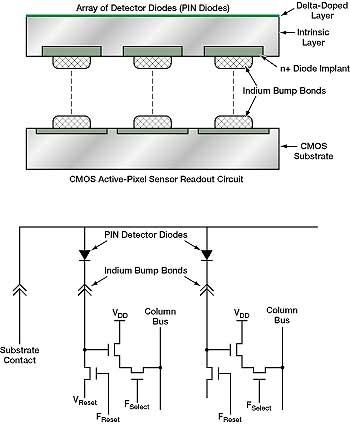
The detector would be a hybrid of (1) a square array of reverse-biased positive/intrinsic/negative (PIN) diodes with (2) a correspondingly patterned complementary metal oxide/semiconductor (CMOS) integrated readout circuit fabricated by a standard process. The array of PIN diodes would be electrically and mechanically connected to the readout circuit through indium bump bonds (see figure).
In a reverse-biased PIN diode, the applied electric field depletes the intrinsic region of charge carriers. When an energetic charged particle or photon of sufficient energy enters the depletion region, some or all of its energy is dissipated in the generation of electron/ hole pairs, which are then swept out by the electric field and detected. However, low-energy particles typically do not penetrate to the intrinsic region in a conventional PIN diode. Instead, they tend to dissipate their energies in a "dead" layer near the surface through which they enter. The dead layer contains an undepleted, highly p- or n-doped, diode contact sublayer where electrons and holes recombine before they can be detected. The dead layer also contains a surface depletion sublayer with an electric field that (a) tends to confine some charge carriers until they recombine at the surface and (b) drives other charge carriers into the undepleted region, where they recombine before detection.
The delta-doping aspect of the delta-doped hybrid advanced detector would extend the low-energy detection limit by reducing the effect of the dead layer. Delta doping is so named because its density-vs.-depth characteristic is reminiscent of the Dirac d function (impulse function). The dopant is concentrated in a very thin layer (preferably, a single atomic layer). In the delta-doped hybrid advanced detector, the delta-doped layer would be placed within 5 or 10 Å of the detector surface. The delta-doped layer would provide a very thin undepleted region and surface depletion region, with a resultant dead-layer thickness of only 15 to 20Å, making possible the collection of electrons and holes generated by low-energy charged particles and photons that can penetrate at least 20 Å or so.
Heretofore, delta doping has been used on charge-coupled devices (CCDs). Although CCDs could be used as detectors, they are relatively highly doped; it would be necessary to thin them to enable their charge-collecting depletion regions to extend through the thickness. Thinning can be accomplished only by a difficult fabrication process step, and the remaining thickness is not sufficient for measuring the energies of x rays and high-energy particles that deposit charge carriers at great depths. Accordingly, the array of PIN diodes in the delta-doped hybrid advanced detector are made from a wafer of high-resistivity silicon [nominally intrinsic, though actually very lightly p-doped (to a concentration of 1012cm¯3)] like that used in silicon strip detectors. The use of this high-resistivity silicon makes thinning unnecessary, thereby making it possible to retain sufficient thickness for detection of highly energetic charged particles and photons.
The CMOS readout circuit would be of the active-pixel sensor (APS) type, offering enough sensitivity to enable resolution of the small signals generated by low-energy charged particles. This circuit would consume only milliwatts of power, in contradistinction to a CCD, which typically consumes watts. Moreover, whereas a CCD must be read out sequentially by rows and columns, the APS circuit would be capable of nonsequential readout of pixels, making it possible to use various advanced readout schemes. Like a CCD, this readout circuit could preserve the low capacitance of the detector diodes, with resultant readout noise of 10 electrons or less (vs. hundreds to thousands of electrons for a conventional strip detector).
A pixel-guarding technique would be used to preserve low effective input capacitances for the APS readout circuit, even in the presence of relatively large indium bump pads on the input nodes, thereby preserving the high conversion gain needed for high sensitivity and a high signal-to-noise ratio. In this technique, each bump bond would be connected to a source follower serving as a unity-gain buffer, the output of which would be fed to a metal guard electrode underneath the bump bond and separated from the bump bond by a thin insulating layer.
This work was done by Eric Fossum, Thomas Cunningham, Shouleh Nikzad, George Soli, and Bedabrata Pain of Caltech for NASA's Jet Propulsion Laboratory. In accordance with Public Law 96-517, the contractor has elected to retain title to this invention. Inquiries concerning rights for its commercial use should be addressed to
Technology Reporting Office
JPL
Mail Stop 122-116
4800 Oak Grove Drive
Pasadena, CA 91109
(818) 354-2240
Refer to NPO-20111
This Brief includes a Technical Support Package (TSP).
Delta-doped hybrid advanced detector
(reference NPO20111) is currently available for download from the TSP library.
Don't have an account?
Overview
The document discusses the Delta-Doped Hybrid Advanced Detector, a novel technology developed to enhance the detection of low energy particles, such as protons and electrons, as well as high energy particles and photons across a wide energy spectrum. Traditional silicon detectors face challenges in detecting low energy particles due to surface fields that can neutralize charge clouds generated near the surface, leading to inadequate signal collection. Additionally, conventional readout schemes are often too noisy and slow for effective energy resolution.
The proposed solution combines several advanced technologies to create a more effective detection system. The detector utilizes a delta-doping scheme, which involves placing a highly doped layer at the surface to terminate surface drift fields, allowing for better charge collection from low energy particles. Unlike traditional charge-coupled devices (CCDs), this hybrid detector employs a high resistivity bulk, eliminating the need for thinning the silicon material, which can be a complex and costly process.
Key features of the detector include a diode array formed from high resistivity silicon, which generates electron-hole pairs when high energy particles pass through. The readout mechanism is based on a CMOS Active Pixel Sensor (APS), which offers low power consumption and a flexible readout scheme compared to the strictly sequential readout of CCDs. This APS readout can achieve a read noise of 10 electrons or less, significantly improving sensitivity and signal-to-noise ratio.
The document also describes a new pixel guarding technique that reduces input capacitance on the APS readout, preserving high conversion gain and enhancing overall sensitivity. By integrating these innovations, the Delta-Doped Hybrid Advanced Detector is expected to extend the low energy detection limit from about 10 keV down to hundreds of eV while maintaining the ability to detect high energy particles beyond MeV.
In summary, this advanced detector is poised to revolutionize particle detection by providing high sensitivity, low power consumption, and the capability to detect a wide range of energies, from visible light to hard X-rays. The technology is currently under development, with potential applications in various fields, including space exploration and high-energy physics.