
Efforts are under way to develop back-surface-illuminated, thinned silicon charge-coupled devices (CCDs) with delta doping and integral optical filters to be used as image detectors in the ultraviolet wavelength range. The concept of delta doping of back-surface-illuminated, thinned silicon CCDs as part of an overall design to make CCDs sensitive to ultraviolet light is not new in itself. Delta-doped CCDs were invented at NASA's Jet Propulsion Laboratory in 1992, and it is well established that this process produces ultraviolet-sensitive CCDs with stable and uniform 100-percent internal quantum efficiency. The novelty lies in the proposed fabrication of such CCDs in which both delta doping and optical filter layers would be deposited as integral parts of unitary device structures.
Because silicon CCDs are sensitive to visible light, one of the major challenges in the development of ultraviolet imaging CCDs is to satisfy the need for filters that will reject visible light but pass ultraviolet light. Another major challenge is posed by the fact that the naturally-formed SiO2 on the air-exposed Si surfaces absorbs light strongly at wavelengths < 140 nm. Hence, it would be desirable to eliminate the SiO2 layers as well as to deposit visible-light-rejecting filters and antireflection layers on the back surfaces of the CCDs.
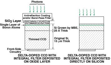
The use of integral filters (as distinguished from external filters that are fabricated on separate substrates) would (1) increase the robustness of image detectors by eliminating the external filters, which are delicate; (2) eliminate the need for structural supports for the filters; (3) eliminate the need for the substrates on which external filters are constructed and which introduce optical losses that degrade detector responses at short wavelengths; and (4) reduce the number of optical surfaces, thereby reducing overall optical losses by eliminating the loss (typically at least 2 to 3 percent) associated with each such surface eliminated.
Because the delta-doped layer lies permanently ~5-10 Å beneath the back surface of a CCD, the delta doping process does not pose an impediment to the subsequent deposition of optical filters and antireflection layers. The problem then becomes one of depositing these optical layers directly on the silicon surface, without the formation of an intervening SiO2layer. The approach taken in the present development effort is to perform delta doping in one ultrahigh-vacuum molecular-beam epitaxy (MBE) chamber and then, without breaking vacuum, transfer the CCD to a connected metal/insulator MBE chamber wherein the filter layers are deposited. By refraining from breaking vacuum until after the deposition of the filter layers, one can prevent the formation of the SiO2 layer (see figure). At the time of reporting the information for this article, MgF2 antireflection layers optimized for the wavelength range of 200 to 300 nm had been deposited on delta-doped CCDs and were found to result in a modest increase in the quantum efficiency of the CCDs at a wavelength of 180 nm.
This work was done by Shouleh Nikzad, Peter Deelman, Paula Grunthaner, Frank Grunthaner, Michael Hoenk, and R.W. Terhune of Caltech forNASA's Jet Propulsion Laboratory.
In accordance with Public Law 96-517, the contractor has elected to retain title to this invention. Inquiries concerning rights for its commercial use should be addressed to
Intellectual Property group
JPL
Mail Stop 202-233
4800 Oak Grove Drive
Pasadena, CA 91109
(818) 354-2240
Refer to NPO-21007
This Brief includes a Technical Support Package (TSP).
Back-Illuminated CCDs with Integral Ultraviolet-Pass Filters
(reference NPO21007) is currently available for download from the TSP library.
Don't have an account?
Overview
The document is a technical support package from NASA detailing advancements in delta-doped charge-coupled devices (CCDs) with integrated ultraviolet (UV) coatings. It is authored by a team from the Jet Propulsion Laboratory (JPL) and highlights the challenges and solutions associated with enhancing CCD sensitivity to UV light, which is crucial for astronomical observations.
CCDs are traditionally not sensitive to UV light, but the document discusses methods to treat them for improved UV response. One significant issue in UV astronomy is the interference from visible light, which can overwhelm the weaker UV signals from astronomical sources. The document emphasizes the need for filters that can effectively block visible wavelengths while allowing UV light to pass through. Delta-doped CCDs are noted for their compatibility with in situ filter deposition, which can enhance their performance in capturing UV light, particularly in the 100 to 200 nm wavelength range.
The document outlines the advantages of integrating UV-pass filters directly onto the CCDs. This integration is essential for applications requiring high sensitivity to UV wavelengths, such as detecting the Lyman-alpha line, which is important in various astronomical studies. The native silicon dioxide surface layer of CCDs becomes strongly absorbing at these wavelengths, making the integration of filters even more critical.
Additionally, the document acknowledges the collaborative nature of the research, funded by NASA's Office of Space Science and other organizations. It highlights the potential applications of this technology in space exploration and scientific imaging, where enhanced UV sensitivity can lead to better data collection and analysis of celestial phenomena.
Overall, the document serves as a comprehensive overview of the development and implications of delta-doped CCDs with UV coatings, showcasing the innovative approaches taken to overcome technological hurdles in UV-sensitive imaging. It reflects the ongoing efforts in space microelectronics technology to improve observational capabilities in astronomy and related fields.