
Curved-focal-plane arrays of back-illuminated silicon-based photodetectors are being developed. The basic idea is to improve the performance of an imaging instrument and simplify the optics needed to obtain a given level of performance by making an image sensor (e.g., a photographic film or an array of photodetectors) conform to a curved focal surface, instead of following the customary practice of designing the optics to project an image onto a flat focal surface. Eyes are natural examples of optical systems that have curved focal surfaces on which image sensors (retinas) are located.
One prior approach to implementation of this concept involves the use of curved-input-surface microchannel plates as arrays of photodetectors. In comparison with microchannel plates, these curved-focal-plane arrays would weigh less, operate at much lower voltages, and consume less power. It should also be possible to fabricate the proposed devices at lower cost.
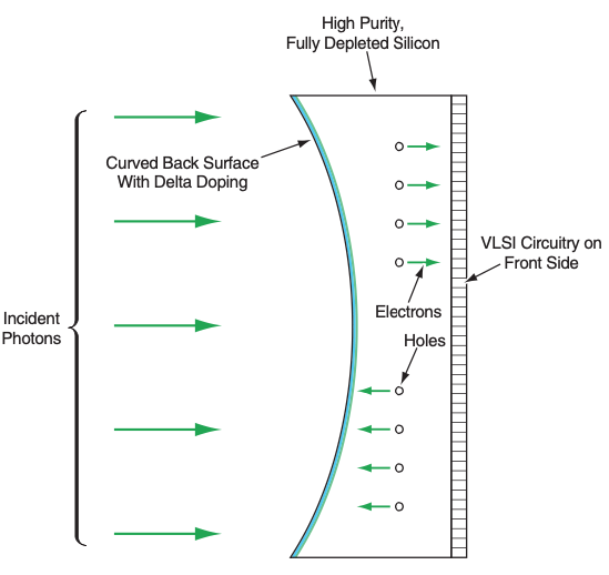
It would be possible to fabricate an array of photodetectors and readout circuitry in the form of a very-large-scale integrated (VLSI) circuit on a curved focal surface, but it would be difficult and expensive to do so. In a simple and inexpensive alternate approach, a device (see figure) would have (1) a curved back surface, onto which light would be focused; and (2) a flat front surface, on which VLSI circuitry would be fabricated by techniques that are well established for flat surfaces.
The device would be made from ultrapure silicon, in which it is possible to form high-resistivity, thick photodetectors that are fully depleted through their thicknesses. (As used here, "thick" means having a thickness between a fraction of a millimeter and a few millimeters.) The back surface would be polished to the curvature of the focal surface of the intended application. To enable the collection of charge carriers excited by photons near the back surface or in the bulk of the device, it would be necessary to form a transparent or semitransparent back-surface electrode, possibly by delta doping. [Delta doping is so named because its density-vs.-depth characteristic is reminiscent of the Dirac d function (impulse function): the dopant is concentrated in a very thin layer - nominally, a single atomic layer.]
This work was done by Shouleh Nikzad and Michael E. Hoenk of Caltech for NASA's Jet Propulsion Laboratory.
In accordance with Public Law 96-517, the contractor has elected to retain title to this invention. Inquiries concerning rights for its commercial use should be addressed to
Intellectual Assets Office
JPL
Mail Stop 202-233
4800 Oak Grove Drive
Pasadena, CA 91109
(818) 354-2240
E-mail: This email address is being protected from spambots. You need JavaScript enabled to view it.
Refer to NPO-30566.
This Brief includes a Technical Support Package (TSP).
Curved Focal-Plane Arrays Using Back-Illuminated High-Purity Photodetectors
(reference NPO30566) is currently available for download from the TSP library.
Don't have an account?
Overview
The document discusses the development of curved focal plane arrays (CFPAs) using polished back-illuminated high-resistivity detectors, a project undertaken by Michael E. Hoenk and Shouleh Nikzad at NASA's Jet Propulsion Laboratory (JPL). The innovation aims to simplify the design of optical systems for space missions by creating detectors that conform to the naturally curved focal surfaces of optical systems, thereby eliminating the need for additional optical elements that typically flatten these surfaces.
High-resistivity detectors are made from ultra-pure silicon, allowing them to be fully depleted through their thickness, which ranges from fractions of a millimeter to several millimeters. The back surface of these detectors can be polished to achieve the desired curvature, facilitating the collection of charge carriers generated by photons. This is achieved through techniques such as delta doping, which involves concentrating dopants in a thin layer to form a transparent or semi-transparent back-surface electrode.
The document highlights the advantages of using curved focal plane arrays, including reduced size, weight, and complexity of optical systems, which are critical for NASA's vision of smaller, more frequent missions. By aligning the detector's curvature with the optical system's focal surface, the design can avoid the complications and penalties associated with traditional flat detector arrays, such as increased mass and cost. This approach is particularly beneficial for long-range space exploration missions where efficiency and cost-effectiveness are paramount.
The document also references specific applications where this technology could be advantageous, such as in wide-field rover cameras, star tracker cameras, and far ultraviolet instruments. The authors emphasize that the simplification of optical designs through the use of CFPAs could be mission-enabling, allowing for more effective and efficient space exploration.
In summary, the document presents a novel approach to the fabrication of curved focal plane arrays that leverages high-resistivity silicon detectors, promising significant improvements in the design and performance of optical systems for space missions. This innovation aligns with NASA's goals of enhancing mission capabilities while minimizing costs and complexities.