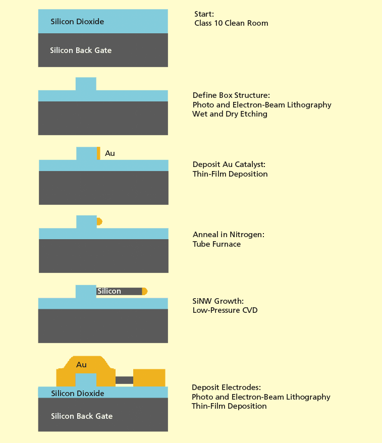
It is now possible to grow silicon nanowires at chosen positions and orientations by a method that involves a combination of standard microfabrication processes. Because their positions and orientations can be chosen with unprecedented precision, the nanowires can be utilized as integral parts of individually electronically addressable devices in dense arrays.

The method involves formation of metal catalytic particles at the desired positions on a substrate, followed by heating the substrate in the presence of silane gas. The figure illustrates an example in which a substrate includes a silicon dioxide surface layer that has been etched into an array of pillars and the catalytic (in this case, gold) particles have been placed on the right-facing sides of the pillars. The catalytic thermal decomposition of the silane to silicon and hydrogen causes silicon columns (the desired nanowires) to grow outward from the originally catalyzed spots on the substrate, carrying the catalytic particles at their tips. Thus, the position and orientation of each silicon nanowire is determined by the position of its originally catalyzed spot on the substrate surface, and the orientation of the nanowire is perpendicular to the substrate surface at the originally catalyzed spot.
The diameter of the nanowire is determined by the diameter of its catalytic particle. In principle, using this technique, the diameter of the silicon nanowire can be controlled precisely by the dimensions of the surface pillar. In the example of the figure, the positions and diameter of the catalytic particles are determined as follows: The right-facing pillar surfaces are coated with gold in a directional evaporative deposition process. The deposition thickness is chosen in conjunction with the area of the pillar faces so that the amount of gold on each face is such that if the gold were aggregated into a hemisphere at the center of each face, the diameter of the hemisphere would equal the desired diameter of the nanowires to be grown from the pillar faces. The aggregation is effected by heating the workpiece in an inert atmosphere.
The pillar array can then be used as a reference mark for straightforward device fabrication in a process called alignment. Knowing the position of the silicon nanowires avoids the present difficulties of working with random or semi-random distributions of silicon nanowires. In an important class of potential applications, nanobridges would be coated with biomolecules (e.g., antigens) that bind to other biomolecules of interest (e.g., the antibodies corresponding to the antigens) to enable highly sensitive detection of the molecules of interest. Sensors comprising arrays of multiplexed nanobridges functionalized for detection of proteins symptomatic of cancer have already been demonstrated to be feasible.
This work was done by Stephanie A Getty of Goddard Space Flight Center. GSC-15368-1

