Reactive-ion etching (RIE) under conditions described below has been found to be a suitable means for patterning piezoelectric thin films made from such materials as PbZr1-xTixO3 or BaxSr1-xTiO3. In the original application for which this particular RIE process was developed, PbZr1-xTixO3 films 0.5 μm thick are to be sandwiched between Pt electrode layers 0.1 µm thick and Ir electrode layers 0.1 μm thick to form piezoelectric capacitor structures. Such structures are typical of piezoelectric actuators in advanced microelectromechanical systems now under development or planned to be developed in the near future.
RIE of PbZr1-xTixO3 is usually considered to involve two major subprocesses: an ion-assisted-etching reaction, and a sputtering subprocess that removes reactive byproducts. RIE is favored over other etching techniques because it offers a potential for a high degree of anisotropy, high-resolution pattern definition, and good process control. However, conventional RIE is not ideal for patterning PbZr1-xTixO3 films at a thickness as great as that in the original intended application. In order to realize the potential benefits mentioned above, it is necessary to optimize process conditions — in particular, the composition of the etching gas and the values of such other process parameters as radio-frequency power, gas pressure, gas-flow rate, and duration of the process. Guidelines for determining optimum conditions can be obtained from experimental determination of etch rates as functions of these parameters.
Etch-gas mixtures of BCl3 and Cl2, some also including Ar, have been found to offer a high degree of selectivity as needed for patterning of PbZr1-xTixO3 films on top of Ir electrode layers in thin-film capacitor structures. The selectivity is characterized by a ratio of Å10:1 (rate of etching PbZr1-xTixO3 ÷ rate of etching Ir and IrOx). At the time of reporting the information for this article, several experiments on RIE in BCl3 and Cl2 (and sometimes Ar) had demonstrated the 10:1 selectivity ratio, and further experiments to enhance understanding and obtain further guidance for optimizing process conditions were planned.
This work was done by Eui-Hyeok Yang and Larry Wild of Caltech for NASA's Jet Propulsion Laboratory. For further information, access the Technical Support Package (TSP) free on-line at www.techbriefs.com/tsp under the Manufacturing category.
In accordance with Public Law 96-517, the contractor has elected to retain title to this invention. Inquiries concerning rights for its commercial use should be addressed to:
Intellectual Assets Office
JPL
Mail Stop 202-233
4800 Oak Grove Drive
Pasadena, CA 91109
(818) 354-2240
E-mail:
Refer to NPO-30349, volume and number of this NASA Tech Briefs issue, and the page number.
This Brief includes a Technical Support Package (TSP).

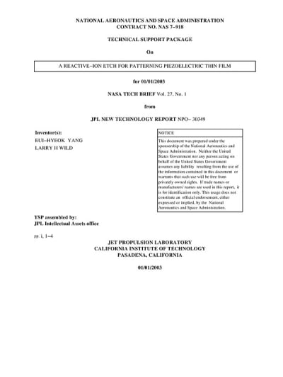
A Reactive-Ion Etch for Patterning Piezoelectric Thin Film
(reference NPO-30349) is currently available for download from the TSP library.
Don't have an account?
Overview
The document presents a technical support package from NASA detailing a reactive-ion etching (RIE) process specifically designed for patterning piezoelectric thin films, such as PbZr1–xTixO3 (PZT) and BaxSr1–xTiO3 (BST). These materials are critical in the development of advanced microelectromechanical systems (MEMS), particularly for applications involving piezoelectric actuators.
The etching of ferroelectric thin films has traditionally relied on chemical wet etching methods. However, recent advancements have shifted focus towards dry etching techniques, including ion beam etching, plasma etching, and RIE. RIE is particularly favored due to its potential for high anisotropy, resolution, and process control. Despite these advantages, conventional RIE methods face challenges when etching thicker films (around 1 μm), as they often exhibit poor selectivity for common masking materials like photoresist and platinum (Pt).
The document highlights the development of a new RIE process that utilizes a gas combination of BCl3 and Cl2, achieving a high selectivity etch ratio of 10:1. This improvement addresses the limitations of previous gas combinations, which resulted in low etch rates and inadequate selectivity. The authors emphasize the importance of optimizing etching conditions, including radio-frequency power, gas pressure, gas flow rate, and gas composition, to enhance the etching performance.
The technical disclosure outlines the motivation behind this innovation, which stems from the growing interest in ferroelectric thin films due to their significant piezoelectric properties. The document also discusses the experimental determination of etch rates as a function of various parameters, providing guidelines for achieving optimal etching conditions.
In summary, this NASA technical brief details a novel RIE process for patterning piezoelectric thin films, addressing key challenges in the fabrication of piezoelectric capacitors. The findings contribute to the advancement of MEMS technology, paving the way for improved performance and functionality in future applications. The work was conducted at the Jet Propulsion Laboratory under NASA's sponsorship, underscoring its significance in the field of aerospace and engineering.

