
Voltage glitches are common in a signal chain path, especially when the system is being powered up or down. Depending on the peak amplitude and glitch duration, the end result in the system output can be catastrophic. One example is an industrial motor control system where a digital-to-analog converter (DAC) drives the motor drivers to control motor spin. If the glitch amplitude is higher than the motor driver’s sensitivity threshold, the motor could be spinning without control in any direction when the system is powered up/down.
Some causes and solutions were analyzed to reduce power-on/off glitches on a precision DAC buffered output. This brief focuses on the power-on glitch when the DAC output buffer is powered on to voltage output mode. A precision DAC can power on in multiple configurations: zero-scale, mid-scale, or high impedance. The pre-power-off state can be controlled by the user. Some DACs have a built-in power-on glitch reduction (POGR) circuit that holds the DAC’s output stage in a configuration where the DAC output stage is not being driven. Buffered voltage-output DACs have a pair of PFET and NFET as the output stage. The POGR circuit disables the PFET and biasing the NFET above its threshold voltage (VTH), minimizing the power-on glitch to a few 100 mV.
The POGR circuit is not present in every DAC. For DACs without POGR, the power-on/off glitch depends upon multiple factors:
- DAC’s power-on state to voltage output mode and high-impedance mode
- Power-on sequence of other supply pins such as the DVDD, VREF, IOVDD, and others
- Feedback network connections
- Power supply ramp rate
- Output resistive load
This article addresses the case where the output stage is powered on to voltage output mode. In this mode, the gate of PFET and NFET are controlled via a pre-output stage. The pre-output stage requires a certain minimum voltage to start functioning correctly. This voltage is also known as the minimum headroom (VH). This voltage depends on the pre-output stage architecture and can be as high as 6V. This voltage is much lower than the minimum supply voltage (VDDMIN) specified in data sheets. Typically, this voltage is not specified in most datasheets.

Before this minimum headroom voltage is reached, the pre-output stage does not have enough headroom to be functional. Therefore, the output FETs gates can be as low as 0V, causing the PFET to behave as a low resistive switch between the supply and output pin as soon as the supply crosses the PFET threshold voltage (VTP). Hence, the output can ramp up with the supply, causing a power-on glitch (see Figure 1).
In this case, the glitch voltage can be as high as the minimum headroom voltage (VH). This glitch is independent of the supply ramp rate because the root cause is insufficient headroom for pre-output stage. All DAC datasheets specify a minimum resistive load (typically 1 kW) at the output. Loading the DAC output with a resistive load is a common technique to minimize this glitch. However, this technique does not minimize the glitch magnitude, as the output PFET is acting as a switch (or short) between the supply and the output pin. Power-on sequence and feedback network connections can worsen this glitch. Because these factors are often interrelated, both are analyzed as one case.
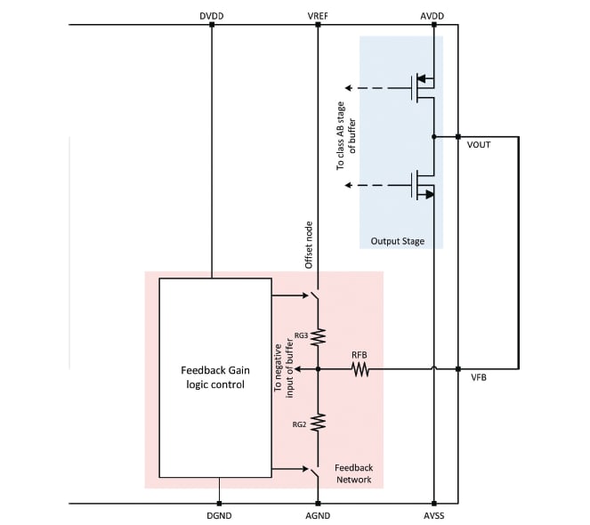
For dual-supply DACs with bipolar outputs, the feedback network also includes an offset node. This node can be driven either by a fixed voltage such as reference pin (VREF), or an offset DAC. The offset DAC is useful when the user requires offsetting the output by a small voltage, allowing for an asymmetrical output range; for example, from –5V to +10V.
Figure 2 is a simplified diagram of an output stage with feedback network. This feedback network requires switches to alter the DAC’s gain and offset. These switches are powered from a separate digital supply, or DVDD. Depending on the DVDD’s power-on sequence, the gain/offset path could be open or shorted to the VREF/AGND pin. This could result in an erroneous gain setting during startup and contribute to the power-on glitch. In most multiple-supply DACs, a certain power-on sequence is recommended to avoid this situation.
Power-on glitches do not depend on the state of DAC registers. All DAC registers are held in reset state while the DAC powers up by a circuit called power-on reset (POR). By the time these registers are released from the reset state, the output and pre-output stages have enough headroom to function correctly.
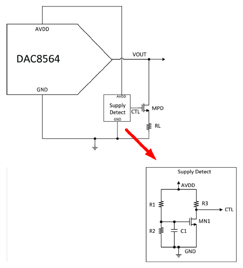
A simple supply detect circuit (Figure 3) can be used to load the DAC’s output momentarily during supply ramp-up. The DAC output VOUT is loaded with resistor RL during the supply ramp-up via FET MPD. The supply-detect block generates the MPD control. During the supply ramp-up, the control signal CTL is pulled to AVDD loading the DAC output VOUT with load RL until the FET MN1 is turned on. After MN1 is completely turned on, it pulls CTL node to ground, unloading the VOUT node. R1, R2, R3, and CL must be sized according to the threshold voltage of MN1.
This article analyzed the power-on glitch and its root causes. While most of the analysis addresses power-on glitches, the same principle applies to power-off glitches. Certain DACs power on in normal mode with no internal POGR circuit. A small resistive load between the output pin and ground during startup is the only way to minimize the power-on glitch of these DACs.
This work was done by Rahul Prakash, Electrical Design Engineer, and Eugenio Mejia, Electrical Applications Engineer at Texas Instruments, Dallas, TX. For more information, Click Here . Contact Rahul Prakash at