
An effort is underway to develop processes for making templates that could be used as deposition molds and etching masks in the fabrication of devices containing arrays of nanowires and/or nanoconduits. Examples of such devices include thermoelectric devices, nerve guidance scaffolds for nerve repair, photonic-band-gap devices, filters for trapping microscopic particles suspended in liquids, microfluidic devices, and size-selective chemical sensors. The technology is an extension of previous work conducted by JPL, UCSD (University of California, San Diego), and Paradigm Optics Inc., which developed a process to fabricate macroporous scaffolds for spinal-cord repair.
 Highly-ordered, optical-fiber arrays consisting of dissimilar polymers comprise the template technology. The selective removal of the fiber cores in specific solvents creates the porous templates to be filled with a “top-down” deposition process such as electrochemical deposition, sputter deposition, molecular beam epitaxy, and the like.
Typically, the fiber bundles consist of polystyrene (PS) fiber cores, which are clad with varying thickness poly(methyl methacrylate) (PMMA). When arranged in hexagonal, close packed configuration and pulled, the fibers form highly ordered arrays comprised of PS fiber cores surrounded by a continuous matrix of PMMA. The ratio of PMMA cladding thickness to PS core diameter determines the spacing between PS fiber cores and typically ranges from 3:1 to 1:1.
 Essentially, the simultaneous heating and drawing or pulling in the longitudinal direction of polymer-fiber arrays fuses the fibers together. Since the fusing process is a constant volume process, a lateral or cross section reduction is accompanied by a commensurate increase in length. Thus, the degree of pulling determines the final core dimensions.
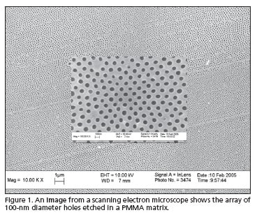
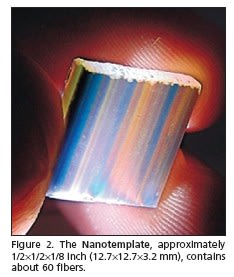
Compared to previous work, where the fiber cores were in the range of 100 to 200 microns, the extent of pulling was significantly increased, thus resulting in a significant reduction in feature dimensions. The scanning electron microscope (Figure 1) image reveals the close packed array 100-nm diameter holes etched in a PMMA matrix (center image). The background image indicates that the hole monodispersity and order is maintained over relatively large areas. The original template length or fiber length was greater than 1 cm and the cross sectional dimension was 1 cm by 0.4 cm (Figure 2). In principle, the depth of the holes could be far greater than 1 mm, which could result in features with aspect ratios (length/diameter) in the 1,000 to 10,000 range.
This work was done by Jeffrey Sakamoto of Caltech for NASA’s Jet Propulsion Laboratory, and Todd Holt and David Welker of Paradigm Optics, Inc. For further information, access the Technical Support Package (TSP) free on-line at ww.techbriefs.com/tsp under the Manufacturing & Prototyping category. In accordance with Public Law 96-517, the contractor has elected to retain title to this invention. Inquiries concerning rights for its commercial use should be addressed to
: Innovative Technology Assets Management JPL Mail Stop 202-233 4800 Oak Grove Drive Pasadena
CA 91109-8099 (818) 354-2240
Refer to NPO-41906, volume and number of this NASA Tech Briefs issue, and the page number.
This Brief includes a Technical Support Package (TSP).
Templates for Fabricating Nanowire/Nanoconduit-Based Devices
(reference NPO-41906) is currently available for download from the TSP library.
Don't have an account?
Overview
The document titled "Templates for Fabricating Nanowire/Nanoconduit-Based Devices" from NASA's Jet Propulsion Laboratory outlines a novel and economical process for creating devices using ordered nanowire arrays. This technology builds upon previous work at JPL, which involved fabricating nerve guidance scaffolds for spinal cord repair using BiComponent Polymer Fiber Matrix (BCPFM) templates. The new approach allows for the creation of templates with significantly smaller pores, potentially achieving diameters below 10 nanometers, making it suitable for fabricating nanoscale elements like nanowires.
The proposed polymer-based technology stands out among existing methods for nanowire fabrication due to its unique attributes. It is capable of producing nanowires or nanoconduits that can reach lengths of centimeters, which is not achievable with other techniques. The introduction of a third compatible polymer system enables the fabrication of multicomponent polymer fiber templates, allowing for the selective deposition of different materials in well-defined arrays. This capability is particularly beneficial for creating devices that require dissimilar materials, such as thermoelectrics and semiconductor devices with both positive and negative electrodes.
The document also discusses the various established methods for fabricating nanowires, including anodized alumina, block copolymers, track-etched polymer membranes, and nanochannel glass. It emphasizes that while there are over ten methods available, the proposed technology offers distinct advantages, particularly in terms of integration with existing technologies in which the authors have significant experience, such as biopolymer structures, sensors, and optical devices.
Additionally, the report highlights the intriguing physical properties of nanowires, which arise from their nanoscale dimensions, including thermoelectric, electronic, magnetic, and mechanical characteristics. It lists potential applications for nanowire-based technologies, including field-effect transistors, diodes, LEDs, microfluidic devices, photonic bandgap devices, and various sensors.
Overall, this document serves as a comprehensive overview of a promising new technology for nanowire fabrication, detailing its unique benefits, potential applications, and the broader implications for advancements in nanotechnology and related fields.