
A recent collaboration between the Whitesides Group at Harvard University and CSM Instruments has culminated in an important advance in lithography of different materials at the nano scale. The motivation for this
development was the ability to produce unique lithographical patterns of different shapes and sizes for use in research applications, such as lab-on-a-chip, where conventional techniques such as electron-beam lithography (EBL) and photolithography cannot be used.
- It can generate multiple levels of relief (height) by altering the applied load.
- It can control the shape of the pattern by using indenters of different shapes.
- It can produce patterns in very hard materials if a diamond indenter is used.
- It can produce features with a wide range of depths, from a few to several hundred nanometers.
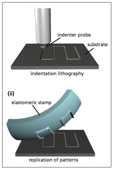
These characteristics produce patterns with three-dimensional relief, which would be impossible to achieve using lithographic techniques in which features have a fixed depth and approximately vertical sidewalls. Resultant patterns can then be replicated as shown in Figure 1 to produce a stamp bearing an inverse replica of the original pattern. Such replicas can in turn be used to pattern other materials in an efficient and cost-effective manner.

The actual shape of the patterns is achieved with a Physik Instrumente (PI) P-733.2CD stage, which is mounted directly on the Open Platform, and allows sub-nanometer positioning resolution in the X and Y axes.
The combination of nanopositioning, accurate load control, and choice of indenter geometry means that almost any shape and depth of feature can be achieved in a fast and reproducible manner.
This work was done by Jinlong Gong, Darren J. Lipomi, Jiangdong Deng, Zhihong Nie, Xin Chen, Nicholas X. Randall, and George M. Whitesides of Harvard University; and Rahul Nair of CSM Instruments. For more information, Click Here .