
A method of fabrication of wires having micron and submicron dimensions is built around electrochemical deposition of the wires in their final positions between electrodes in integrated circuits or other devices in which the wires are to be used. Heretofore, nanowires have been fabricated by a variety of techniques characterized by low degrees of controllability and low throughput rates, and it has been necessary to align and electrically connect the wires in their final positions by use of sophisticated equipment in expensive and tedious post-growth assembly processes. The present method is more economical, offers higher yields, enables control of wire widths, and eliminates the need for post-growth assembly. The wires fabricated by this method could be used as simple electrical conductors or as transducers in sensors. Depending upon electrodeposition conditions and the compositions of the electroplating solutions in specific applications, the wires could be made of metals, alloys, metal oxides, semiconductors, or electrically conductive polymers.
In this method, one uses fabrication processes that are standard in the semiconductor industry. These include cleaning, dry etching, low-pressure chemical vapor deposition, lithography, dielectric deposition, electron-beam lithography, and metallization processes as well as the electrochemical deposition process used to form the wires. In a typical case of fabrication of a circuit that includes electrodes between which microscopic wires are to be formed on a silicon substrate, the fabrication processes follow a standard sequence until just before the fabrication of the microscopic wires.
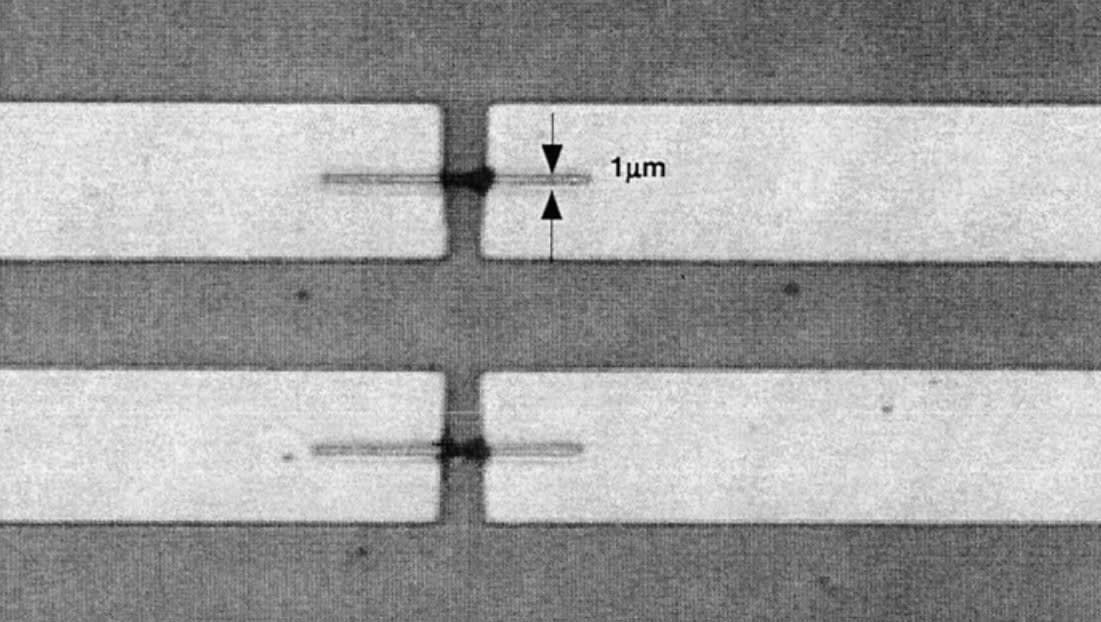
Then, by use of a thermal SiO-deposition technique, the electrodes and the substrate surface areas in the gaps between them are covered with SiO. Next, the SiO is electron-beam patterned, then reactive-ion etched to form channels having specified widths (typically about 1 µm or less) that define the widths of the wires to be formed. Drops of an electroplating solution are placed on the substrate in the regions containing the channels thus formed, then the wires are electrodeposited from the solution onto the exposed portions of the electrodes and into the channels. The electrodeposition is a room-temperature, atmospheric-pressure process. The figure shows an example of palladium wires that were electrodeposited into 1-mm wide channels between gold electrodes.
This work was done by Minhee Yun, Nosang Myung, and Richard Vasquez of Caltech for NASA’s Jet Propulsion Laboratory. For further information, access the Technical Support Package (TSP) free online at www.techbriefs.com/tsp under the Manufacturing category.
In accordance with Public Law 96-517, the contractor has elected to retain title to this invention. Inquiries concerning rights for its commercial use should be addressed to:
Innovative Technology Assets Management
JPL
Mail Stop 202-233
4800 Oak Grove Drive
Pasadena, CA 91109-8099
(818) 354-2240
E-mail: This email address is being protected from spambots. You need JavaScript enabled to view it.
Refer to NPO-40221, volume and number of this NASA Tech Briefs issue, and the page number.
This Brief includes a Technical Support Package (TSP).
In Situ Electrochemical Deposition of Microscopic Wires
(reference NPO-40221) is currently available for download from the TSP library.
Don't have an account?
Overview
The document titled "In Situ Electrochemical Deposition of Microscopic Wires" from NASA's Jet Propulsion Laboratory outlines a novel method for fabricating micron-sized wires with individually addressable capabilities. This technique employs electrochemical deposition in conjunction with standard semiconductor fabrication processes, including metal and dielectric deposition, e-beam lithography, and lithography techniques.
The primary focus of the research is on the synthesis of palladium (Pd) wires, specifically designed to have a diameter of 1 micron and a length of 6 microns. The fabrication process begins with the preparation of silicon wafers, which are cleaned and coated with a low-stress silicon nitride layer. Metal films of titanium-gold (Ti-Au) are then deposited to form contact layers, followed by the deposition of silicon oxide (SiO) to create electrolyte channels. The channels are defined using e-beam lithography and reactive-ion etching.
Electrochemical deposition is performed by applying a drop of an electroplating solution containing palladium ions onto the micron channel. The solution is prepared with specific concentrations of palladium and ammonium sulfamate, adjusted to a pH of 8.0. This method allows for the growth of palladium wires with a smooth and directional morphology, which is essential for producing nanowires with minimal dimensions.
The document emphasizes the advantages of this direct growth method, which operates at room temperature and ambient pressure, making it cost-effective and high-yield. The process eliminates the need for complex post-assembly steps, enhancing the efficiency of wire fabrication. The resulting micron-sized wires are stable in both air and aqueous environments, making them suitable for various applications, including nanoelectronic devices and sensors.
Additionally, the method allows for the fabrication of a wide range of sensing materials by varying the electrolyte compositions and deposition conditions. This flexibility opens up possibilities for creating individually addressable nanowire sensor arrays with controlled diameters, which could significantly impact the development of advanced electronic and sensing technologies.
Overall, the document presents a comprehensive overview of a promising technique for the fabrication of microscopic wires, highlighting its potential applications in aerospace and other technological fields.