
A single-chip CMOS-based (complementary-metal-oxide-semi-conductor-based) transmit/receive (T/R) module is being developed for L-band radar systems. Previous T/R module implementations required multiple chips employing different technologies (GaAs, Si, and others) combined with off-chip transmission lines and discrete components including circulators. The new design eliminates the bulky circulator, significantly reducing the size and mass of the T/R module. Compared to multi-chip designs, the single-chip CMOS can be implemented with lower cost. These innovations enable cost-effective realization of advanced phased array and synthetic aperture radar systems that require integration of thousands of T/R modules.
The circulator is a ferromagnetic device that directs the flow of the RF (radio frequency) power during transmission and reception. During transmission, the circulator delivers the transmitted power from the amplifier to the antenna, while preventing it from damaging the sensitive receiver circuitry. During reception, the circulator directs the energy from the antenna to the low-noise amplifier (LNA) while isolating the output of the power amplifier (PA). In principle, a circulator could be replaced by series transistors acting as electronic switches. However, in practice, the integration of conventional series transistors into a T/R chip introduces significant losses and noise.
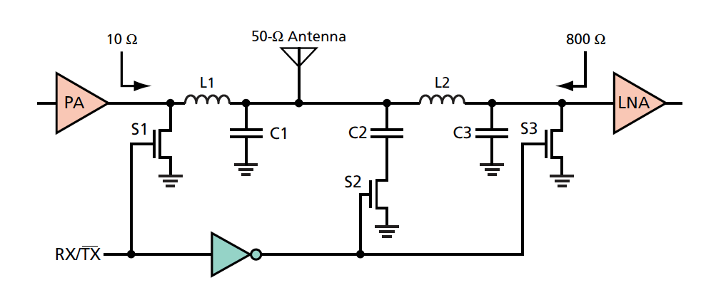
The prototype single-chip T/R module contains integrated transistor switches, but not connected in series; instead, they are connected in a shunt configuration with resonant circuits (see figure). The shunt/resonant circuit topology not only reduces the losses associated with conventional semiconductor switches but also provides beneficial transformation of impedances for the PA and the LNA. It provides full single-pole/double-throw switching for the antenna, isolating the LNA from the transmitted signal and isolating the PA from the received signal. During reception, the voltage on control line RX/TX is high, causing the field-effect transistor (FET) switch S1 to be closed, forming a parallel resonant tank circuit L1||C1. This circuit presents high impedance to the left of the antenna, so that the received signal is coupled to the LNA. At the same time, FET switches S2 and S3 are open, so that C2 is removed from the circuit (except for a small parasitic capacitance). The combination of L2 and C3 forms a matching network that transforms the antenna impedance of 50 ohms to a higher value from the perspective of the LNA input terminal. This transformation of impedance improves LNA noise figure by increasing the received voltage delivered to the input transistor. This allows lower transconductance and therefore a smaller transistor, which makes it possible to design the CMOS LNA for low power consumption. During transmission, the voltage on control line RX/TX is low, causing switch S1 to be open. In this configuration, the combination of L1 and C1 transforms the antenna impedance to a lower value from the perspective of the PA. This low impedance is helpful in producing a relatively high output power compatible with the low CMOS operating potential. At the same time, switches S2 and S3 are closed, forming the parallel resonant tank circuit L2||C2. This circuit presents high impedance to the right of the antenna, directing the PA output signal to the antenna and away from the LNA. During this time, S3 presents a short circuit across the LNA input terminals to guarantee that the voltage seen by the LNA is small enough to prevent damage.
This work was done by Alina Moussessian, Mohammad Mojarradi, Travis Johnson, John Davis, Edwin Grigorian, James Hoffman, and Edward Caro of Caltech; and William Kuhn of Kansas State University for NASA’s Jet Propulsion Laboratory.
In accordance with Public Law 96-517, the contractor has elected to retain title to this invention. Inquiries concerning rights for its commercial use should be addressed to:
Innovative Technology Assets Management
JPL
Mail Stop 202-233
4800 Oak Grove Drive
Pasadena, CA 91109-8099
(818) 354-2240
E-mail: This email address is being protected from spambots. You need JavaScript enabled to view it.
Refer to NPO-40869.
This Brief includes a Technical Support Package (TSP).
Single-Chip T/R Module for 1.2 GHz
(reference NPO-40869) is currently available for download from the TSP library.
Don't have an account?
Overview
The document is a Technical Support Package from NASA's Jet Propulsion Laboratory, detailing the development of a Single-Chip Transmit/Receive (T/R) Module for 1.2 GHz applications. It addresses the challenges and innovations in integrating radar technology into a compact, efficient chip design.
The T/R module is crucial for radar systems, as it facilitates the transmission of signals from a power amplifier (PA) to an antenna and the reception of signals from the antenna to a low-noise amplifier (LNA). Traditional designs often utilize bulky circulators to manage these functions, which can be problematic for integration into a single CMOS chip due to size and performance limitations. The document highlights an alternative approach using a set of integrated shunt resonant switches, which aim to reduce losses and improve the noise figure compared to conventional semiconductor switches.
The design described in the document includes a complete T/R switch solution that provides full Single Pull Double Throw (SPDT) operation. This setup isolates the LNA from the transmit signal and the PA from the receive signal, enhancing performance during both transmission and reception. During receive mode, the circuit presents a high impedance to the antenna, allowing efficient signal steering to the LNA, while during transmit mode, it modifies the antenna impedance to optimize power output.
The document also discusses the challenges of integrating a high-power transmitter within the T/R module. It notes that achieving at least 5W of peak power for each antenna element requires careful impedance matching and power combining, as typical silicon transistors have a breakdown voltage lower than the necessary output levels. Solutions such as transformer arrays and distributed power amplifiers are suggested to address these challenges.
Overall, the document emphasizes the potential of integrating radar functions into a single chip, leveraging the capabilities of CMOS technology. This integration not only simplifies the design but also allows for the incorporation of digital control and power conditioning systems, paving the way for more compact and efficient radar systems in various applications. The insights provided in this document reflect significant advancements in aerospace technology, with implications for broader commercial and scientific uses.