
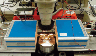
A system of electronic instrumentation, constituting the equivalent of a two-port vector network analyzer, has been developed for use in on-wafer measurement of key electrical characteristics of semiconductor devices at frequencies from 220 to 325 GHz. A prior system designed according to similar principles was reported in "Equipment for On-Wafer Testing at Frequencies Up to 220 GHz" (NPO-20760), NASA Tech Briefs, Vol. 25, No. 11 (November 2001), page 42. As one would expect, a major source of difficulty in progressing to the present higherfrequency- range system was the need for greater mechanical precision as wavelengths shorten into the millimeter range, approaching the scale of mechanical tolerances of prior systems.
This work was done by Lorene Samoska, Alejandro Peralta, Douglas Dawson, and Karen Lee of Caltech; Greg Boll of GGB Industries; and Chuck Oleson of Oleson Microwave Labs for NASA's Jet Propulsion Laboratory. For further information, access the Technical Support Package (TSP) free online at www.techbriefs.com/tsp under the Semiconductors & ICs category. NPO-40955
This Brief includes a Technical Support Package (TSP).
Equipment for On-Wafer Testing From 220 to 325 GHz
(reference NPO-40955) is currently available for download from the TSP library.
Don't have an account?
Overview
The document is a Technical Support Package from NASA's Jet Propulsion Laboratory (JPL), specifically focused on equipment designed for on-wafer testing in the frequency range of 220 to 325 GHz. It is part of NASA Tech Briefs, identified as NPO-40955, and aims to disseminate information about aerospace-related developments that have potential applications beyond their original context.
The document emphasizes the importance of on-wafer testing, which is a critical process in the development and characterization of semiconductor devices, particularly those operating at high frequencies. The ability to test devices directly on the wafer allows for more accurate measurements and can lead to improved performance and reliability in various applications, including telecommunications, radar, and other high-frequency technologies.
Included in the document are figures illustrating the on-wafer measurement system and a WR3 wafer probe, which are essential components for conducting tests in the specified frequency range. These figures provide a visual understanding of the equipment and its configuration, highlighting the technical sophistication involved in high-frequency testing.
The Technical Support Package also serves as a resource for those interested in the broader implications of the technology, encouraging exploration of additional publications and resources available through the NASA Scientific and Technical Information (STI) Program Office. The document provides contact information for the STI Help Desk, offering further assistance and access to a wealth of information related to NASA's research and technology initiatives.
Additionally, the document includes a notice regarding the proprietary nature of the information contained within, indicating that it may be subject to export control regulations. It clarifies that the United States Government, nor any individuals acting on its behalf, assumes liability for the use of the information provided, nor does it guarantee that such use will be free from privately owned rights.
In summary, this Technical Support Package is a valuable resource for understanding the advancements in on-wafer testing technology at high frequencies, showcasing NASA's commitment to sharing knowledge and fostering innovation in aerospace and related fields.