
In a photon counting detector array, each pixel in the array produces an electrical pulse when an incident photon on that pixel is detected. Detection and demodulation of an optical communication signal that modulated the intensity of the optical signal requires counting the number of photon arrivals over a given interval. As the size of photon counting photodetector arrays increases, parallel processing of all the pixels exceeds the resources available in current application-specific integrated circuit (ASIC) and gate array (GA) technology; the desire for a high fill factor in avalanche photodiode (APD) detector arrays also precludes this.
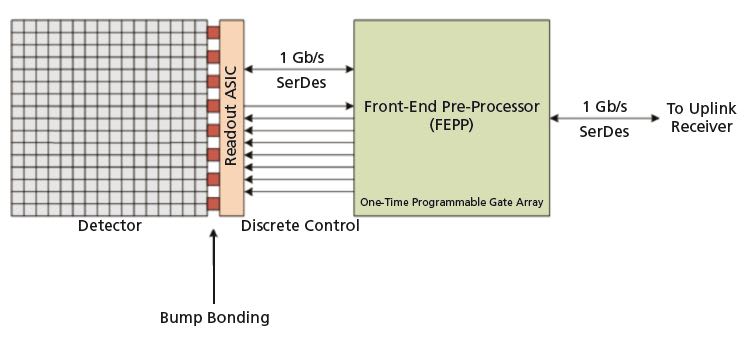
The detector array readout ASIC functions as a parallel-to-serial converter, serializing the photodetector array output for subsequent processing. Additional downsampling functionality for each pixel is added to this ASIC. Due to the large number of pixels in the array, the readout time of the entire photodetector is greater than the time between photon arrivals; therefore, a downsampling pre-processing step is done in order to increase the time allowed for the readout to occur. Each pixel drives a small counter that is incremented at every detected photon arrival or, equivalently, the charge in a storage capacitor is incremented. At the end of a user-configurable counting period (calculated independently from the ASIC), the counters are sampled and cleared. This downsampled photon count information is then sent one counter word at a time to the GA.
For a large array, processing even the downsampled pixel counts exceeds the capabilities of the GA. Windowing of the array, whereby several subsets of pixels are designated for processing, is used to further reduce the computational requirements. The grouping of the designated pixel frame as the photon count information is sent one word at a time to the GA, the aggregation of the pixels in a window can be achieved by selecting only the designated pixel counts from the serial stream of photon counts, thereby obviating the need to store the entire frame of pixel count in the gate array. The pixel count se quence from each window can then be processed, forming lower-rate pixel statistics for each window. By having this processing occur in the GA rather than in the ASIC, future changes to the processing algorithm can be readily implemented.
The high-bandwidth requirements of a photon counting array combined with the properties of the optical modulation being detected by the array present a unique problem that has not been addressed by current CCD or CMOS sensor array solutions.
This work was done by Ferze D. Patawaran, William H. Farr, Danh H. Nguyen, Kevin J. Quirk, and Adit Sahasrabudhe of Caltech for NASA’s Jet Propulsion Laboratory. NPO-48346
This Brief includes a Technical Support Package (TSP).
Downsampling Photodetector Array With Windowing
(reference NPO-48346) is currently available for download from the TSP library.
Don't have an account?
Overview
The document is a Technical Support Package from NASA's Jet Propulsion Laboratory (JPL) that discusses advancements in photodetector technology, specifically focusing on downsampling photodetector arrays with windowing. This technology is part of ongoing research aimed at enhancing optical communications for deep space missions.
The primary goal of the research is to improve data transmission capabilities in deep space, achieving data returns that are 10 to 100 times greater than current radio frequency (RF) communications. This enhancement is crucial for increasing science data return, enabling "virtual presence," and facilitating public engagement through high-definition video and improved imaging resolution for astrophysics and Earth science.
The document outlines the structure of the focal plane array, which consists of both "slow" and "fast" pixels. A sub-array of fast pixels is strategically positioned at the beacon tracking location to optimize performance. The processing of these pixels is critical, as it allows for effective background rate management. The document explains that alternating between "up" and "down" modes in slow counters helps mitigate the impact of background noise, ensuring more accurate data collection.
Additionally, the document discusses the challenges associated with parallel processing of pixel data, which exceeds the capabilities of current application-specific integrated circuits (ASICs) and gate array (GA) technologies. To address these limitations, the research proposes distributing processing tasks across ASICs and GAs through techniques such as downsampling and windowing. This approach allows for efficient data handling and enhances the overall performance of the photodetector array.
The document emphasizes the importance of these advancements in the context of future space exploration, particularly for human exploration beyond low-Earth orbit. The increased resolution and data return capabilities are expected to support the development of advanced instruments and technologies necessary for deep space missions.
In summary, this Technical Support Package highlights JPL's innovative work in optical communications, focusing on the development of photodetector arrays that enhance data transmission capabilities for deep space exploration. The research aims to overcome current technological limitations and pave the way for more effective and engaging scientific missions.