
An improved photodiode-based complementary metal oxide/semiconductor (CMOS) active-pixel sensor (APS) incorporates features to (1) allow imaging with very high electronic shutter speeds, (2) suppress motion artifacts, and (3) prevent image lag and blooming (the spread of image lag to the area adjacent to a brightly illuminated area).
- Motion artifacts are distortions caused by motion in the scene imaged on a sensor. Ordinarily, a CMOS imager of older design is operated in a rolling-shutter mode, in which each row of pixels is exposed at a different instant of time. The rolling-shutter mode introduces distortion into the image; for example, if the scene contains an object moving in the direction of the row exposure sequence, then in the output image, the object appears elongated in the direction of motion.
- Image lag is caused by retention of partial pixel image charges from previous frames. Blooming interferes with efforts to perform high-contrast, low-light imaging.
In the improved CMOS APS, motion artifacts are suppressed by rapid electronic shuttering in a snapshot mode; all pixels are exposed simultaneously. Blooming and image lag are prevented by draining residual pixel photocharges between frames. These improvements are made possible by a unique design implemented in standard single-polysilicon CMOS.
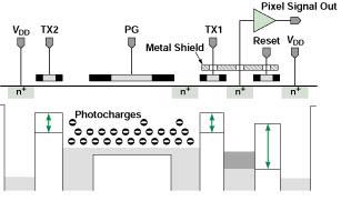
Figure 1 is a schematic cross section of a single-pixel portion of the device. Photocharge is integrated under the photogate (PG). The integration (exposure) time is controlled by a voltage pulse applied to the PG; in general, the exposure time can be thus defined to within 10 µs in this and all other pixels.
There are two transfer gates: TX1 and TX2. The transfer gates are common to the entire CMOS APS chip and are operated by application of voltage pulses timed in conjunction with the voltage pulse applied to the PG. By virtue of fabrication in standard CMOS single-polysilicon CMOS, the gates are separated by floating n+ diffusions. TX1 is used for transferring the integrated photocharge to a sensing node for detection. TX2 serves both as an antiblooming gate and for defining exposure time. The sensing node serves as part of a frame buffer, which makes it possible to perform frame readout at any time after charge integration, independently of the charge-integration time.
Although the exposure time is defined by the duration of the pulse applied to the PG, the floating diffusions continue to collect photocharges. The transfer of these residual photocharges to the sensing node is the cause of image lag in a CMOS APS of older design. In the present CMOS APS, these charges are drained off, prior to beginning integration of charge for the next frame, by application of voltage pulses with suitable timing and levels to the PG and TX2.
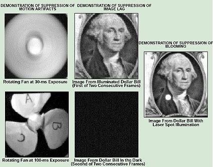
Figure 2 presents some test images acquired by use of the improved CMOS APS:
- Snapshots of a fan rotating at 1,800 revolutions per minute were made with 30-ms and 100-µs exposures. The 100-µs image demonstrates the ability of the device to "freeze" the motion of the fan without introducing motion artifacts.
- Images of George Washington on a dollar bill were made in two consecutive frames with illumination in during the first frame and darkness during the second one. No residual image was observed in the second frame.
- Another image of George Washington on a dollar bill was made with ordinary illumination plus spot illumination by a laser. No blooming was observed, even though the laser illumination was 80 dB above the saturation level of the device.
This work was done by Bedabrata Pain, Guang Yang, Orly Yadid-Pecht, and Chris J. Wrigley of Caltech for NASA's Jet Propulsion Laboratory.
In accordance with Public Law 96-517, the contractor has elected to retain title to this invention. Inquiries concerning rights for its commercial use should be addressed to
Technology Reporting Office
JPL
Mail Stop 122-116
4800 Oak Grove Drive
Pasadena, CA 91109
(818) 354-2240
Refer to NPO-20555
This Brief includes a Technical Support Package (TSP).
Imager with Motion -Artifact Supression and Antiblooming
(reference NPO20555) is currently available for download from the TSP library.
Don't have an account?
Overview
This document presents a technical support package from NASA's Jet Propulsion Laboratory (JPL) detailing advancements in imaging technology, specifically focusing on a novel photodiode-based CMOS active-pixel sensor (APS) designed to suppress motion artifacts and eliminate image lag. The work is attributed to inventors Bedabrata Pain, Guang Yang, Orly Yadid-Pecht, and Christopher J. Wrigley.
The primary innovation lies in the pixel design and timing modifications that allow for high-quality snapshot imaging without the residual image issues commonly associated with traditional CMOS APS. Conventional APS often suffers from image lag due to the retention of photocharges from previous frames, particularly problematic in high-contrast and low-light conditions. The new design incorporates two transfer gates: one for transferring integrated photocharges to the sensing node and another (the blooming gate) for draining unwanted charges. This configuration effectively eliminates residual images while maintaining overall imaging performance.
The document highlights the technical challenges of using rolling shutter modes in CMOS APS, which can lead to motion artifacts when capturing moving images. The proposed solution allows for precise exposure times as short as 10 microseconds, significantly improving the sensor's ability to capture fast-moving subjects without distortion.
Test results indicate that the imager achieves high image quality with low power consumption (only 3 mW at 1 Mpix/sec) and minimal read noise (less than 10 e-). The sensor demonstrates excellent linearity in transfer characteristics and can control exposure down to 90 microseconds. Notably, images captured at high speeds, such as a fan rotating at 1800 RPM, show no motion artifacts, confirming the effectiveness of the technology.
The document also discusses the absence of blooming, even under extreme illumination conditions, and presents experimental results that verify over 74 dB of image lag suppression. The findings suggest that the new imager chip successfully meets the goal of providing high-quality imaging capabilities in a compact, electronically shuttered CMOS design.
In conclusion, this technical support package outlines a significant advancement in imaging technology, showcasing a CMOS APS that effectively addresses common issues like image lag and motion artifacts, paving the way for improved imaging applications in various fields, including aerospace and beyond.