
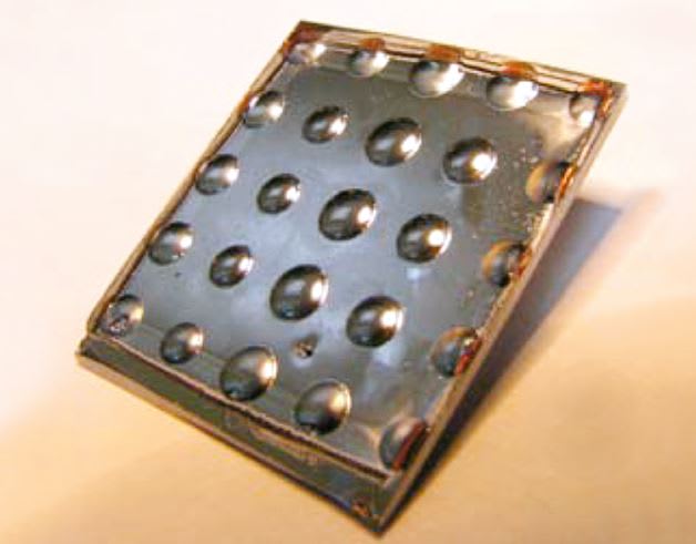
A 5×5 silicon microlens array was developed using a silicon micromachining technique for a silicon-based THz antenna array. The feature of the silicon micromachining technique enables one to microfabricate an unlimited number of microlens arrays at one time with good uniformity on a silicon wafer. This technique will resolve one of the key issues in building a THz camera, which is to integrate antennas in a detector array. The conventional ap proach of building single-pixel receivers and stacking them to form a multi-pixel receiver is not suited at THz because a single-pixel receiver already has difficulty fitting into mass, volume, and power budgets, especially in space applications.
In order to control the curvature of the microlens, the following process variables could be used:
1. Amount of photoresist: It determines the curvature of the photoresist microlens. Since the photoresist lens is transferred onto the silicon substrate, it will directly control the curvature of the silicon microlens.
2. Etching selectivity between photoresist and silicon: The photoresist microlens is formed by thermal reflow. In order to transfer the exact photoresist curvature onto silicon, there needs to be etching selectivity of 1:1 between silicon and photoresist. However, by varying the etching selectivity, one could control the curvature of the silicon microlens.
The figure shows the microfabricated silicon microlens 5×5 array. The diameter of the microlens located in the center is about 2.5 mm. The measured 3-D profile of the microlens surface has a smooth curvature. The measured height of the silicon microlens is about 280 μm. In this case, the original height of the photoresist was 210 μm. The change was due to the etching selectivity of 1.33 between photoresist and silicon. The measured surface roughness of the silicon microlens shows the peak-to-peak surface roughness of less than 0.5 μm, which is adequate in THz frequency. For example, the surface roughness should be less than 7 μm at 600 GHz range. The SEM (scanning electron microscope) image of the microlens confirms the smooth surface. The beam pattern at 550 GHz shows good directivity.
This work was done by Choonsup Lee, Goutam Chattopadhyay, Imran Mehdi, John J. Gill, and Cecile D. Jung-Kubiak of Caltech; and Nuria Llombart of the Universidad Complutense de Madrid, Spain, for NASA’s Jet Propulsion Laboratory.
In accordance with Public Law 96-517, the contractor has elected to retain title to this invention. Inquiries concerning rights for its commercial use should be addressed to:
Innovative Technology Assets Management NPO-48017
JPL
Mail Stop 321-123
4800 Oak Grove Drive
Pasadena, CA 91109-8099
E-mail:
This Brief includes a Technical Support Package (TSP).
Silicon Micromachined Microlens Array for THz Antennas
(reference NPO-48017) is currently available for download from the TSP library.
Don't have an account?
Overview
The document titled "Silicon Micromachined Microlens Array for THz Antennas" is a technical support package from NASA's Jet Propulsion Laboratory (JPL) that outlines advancements in THz (terahertz) technology, specifically focusing on the development of silicon micromachined microlens arrays for THz antennas. The authors, including Choonsup Lee and collaborators from JPL and Universidad Complutense, present a comprehensive overview of the technology's capabilities and applications.
THz technology operates within the frequency range of 3 THz to 300 GHz, with corresponding wavelengths from 0.1 mm to 1 mm. This range is characterized by non-ionizing and non-destructive radiation, making it suitable for various applications, including imaging and sensing. The document highlights the ability of THz waves to penetrate non-conducting materials such as clothing, paper, wood, clouds, and dust, while noting limitations in penetrating water and metals. The technology offers higher spatial resolution compared to traditional RF/mm-wave systems, with a resolution of approximately 0.5 mm.
A significant focus of the document is on the miniaturization of bulky 600 GHz receiver systems through silicon micromachining techniques. The development of silicon microlens antennas is also emphasized, which enhances the performance of THz systems. The document mentions ongoing work on an 8-pixel transceiver, indicating future advancements in the technology.
The technical support package serves as a resource for understanding the broader implications of these developments in aerospace and other fields. It is part of NASA's Commercial Technology Program, aimed at disseminating results from aerospace-related innovations that have potential commercial applications. The document also includes contact information for further inquiries, specifically through the Innovative Technology Assets Management at JPL.
In conclusion, this technical support package provides valuable insights into the advancements in THz technology, particularly through the use of silicon micromachined microlens arrays. It underscores the potential of this technology for various applications while also serving as a resource for further exploration and collaboration in the field.