
Arrays of nanowires having controlled dimensions can now be fabricated on substrates, optionally as integral parts of multilayer structures, by means of a cost-effective, high-yield process based on ion milling on steps. Nanowires made, variously, of semiconductors or metals are needed as components of sensors and high-density electronic circuits.
Unlike prior processes used to fabricate nanowires, the present process does not involve electron-beam lithography, manipulation of nanoscopic objects by use of an atomic-force microscope, or any other technique that is inherently unsuitable for scaling up to mass production. In comparison with the prior processes, this process is rapid and simple. Wires having widths as small as a few tens of nanometers and lengths as long as millimeters have been fabricated by use of this process.
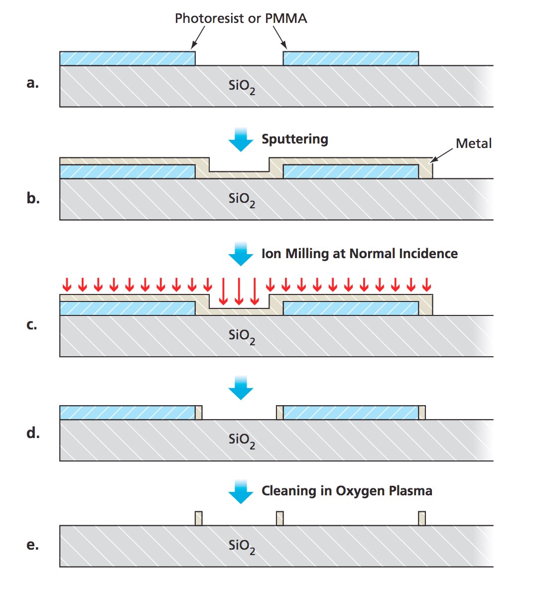
The figure depicts a workpiece at different stages of the process. A silicon dioxide substrate is coated with a photoresist or poly(methyl methacrylate) [PMMA] to a thickness of as much as 500 nm. The photoresist or PMMA is patterned to form edges where wires are to be formed. A metal — either Pt or Ti — is deposited, by sputtering, to a thickness of as much as 200 nm. By ion milling at normal incidence, the thickness of the metal deposit is reduced until the only metal that remains is in the form of wall-like nanowires along the edges of the photoresist or PMMA. Finally, an oxygen plasma is used to remove the photoresist or PMMA, leaving only the nanowires on the substrate.
This work was done by Minhee Yun, Richard Vasquez, and Choonsup Lee of Caltech for NASA's Jet Propulsion Laboratory. For further information, access the Technical Support Package (TSP) free on-line at www.techbriefs.com/tsp under the Manufacturing & Prototyping category. In accordance with Public Law 96-517, the contractor has elected to retain title to this invention. Inquiries concerning rights for its commercial use should be addressed to:
Innovative Technology Assets Management
JPL
Mail Stop 202-233
4800 Oak Grove Drive
Pasadena, CA 91109-8099
(818) 354-2240
E-mail: This email address is being protected from spambots. You need JavaScript enabled to view it.
Refer to NPO-40933, volume and number of this NASA Tech Briefs issue, and the page number.
This Brief includes a Technical Support Package (TSP).
Ion Milling on Steps for Fabrication of Nanowires
(reference NPO-40933) is currently available for download from the TSP library.
Don't have an account?
Overview
The document titled "Ion Milling on Steps for Fabrication of Nanowires" is a Technical Support Package from NASA's Jet Propulsion Laboratory (JPL), detailing a novel technique for nanowire fabrication known as the IMOS (Ion Milling On Step) method. This technique is significant for its potential applications in various technological, scientific, and commercial fields.
The IMOS technique involves several key steps for the effective fabrication of nanowires. Initially, a layer of photoresist (PR) or polymethyl methacrylate (PMMA) is applied, with thicknesses ranging from 100nm to 500nm. Following this, metal sputtering is performed to deposit a metal layer onto the substrate. The process also includes the use of a plasma asher for cleaning the photoresist, ensuring a clean surface for subsequent steps.
The core of the IMOS technique is the ion milling process, where argon ions (Ar+) are utilized to etch away material selectively, leading to the formation of nanowires. This method allows for precise control over the dimensions and shapes of the nanowires, which can be fabricated in sizes as small as 100nm. The document includes illustrations that depict the various stages of the fabrication process, highlighting the transformation from a flat substrate to the final nanowire structures.
The document emphasizes the broader implications of this technology, suggesting that the advancements in nanowire fabrication could lead to significant improvements in electronic devices, sensors, and other applications that require nanoscale components. The research is part of NASA's Commercial Technology Program, aimed at disseminating aerospace-related developments that have wider technological applications.
Additionally, the document provides contact information for further assistance and resources available through NASA's Scientific and Technical Information (STI) Program Office, encouraging interested parties to explore additional publications and research in this area.
In summary, the Technical Support Package outlines a sophisticated method for nanowire fabrication using ion milling, showcasing its potential impact on future technologies and emphasizing NASA's commitment to advancing scientific knowledge and innovation.