
An advanced complementary metal oxide/semiconductor (CMOS) active-pixel sensor (APS) incorporates integrated circuitry that computes the centroid of the image in a window selectable by the user. The development of this circuitry is significant in that it is necessary to compute centroids of images in diverse applications that include robotic vision, autonomous navigation, optical communications, and scientific imaging. Heretofore, it has been necessary to compute centroids by use of off-chip circuitry, at the cost of increased data latency, power consumption, and system size. This circuitry computes image centroids on-chip at a high speed and in analog domain, while consuming little additional power, and is compatible with high-performance CMOS APS circuitry.
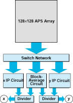
The prototype window-centroiding CMOS APS contains a 128 × 128-pixel APS with its readout circuitry, plus the centroid processor, which includes a switching network, analog inner-product (IP)-computing circuits, and an analog divider (see figure). The centroid computer operates on a window of n × n pixels, where 3 ≤n ≤9 to produce both x and y centroids. Computation of the centroid involves the computation of inner products (weighted sums) and division of the weighted sums by an overall nonweighted sum. Each term in each inner product is proportional to a pixel voltage (which is nominally proportional to pixel brightness) weighted by the integer (between 1 and n, inclusive) that represents the pixel row (y) or column (x) address within the window.
The inner products are computed in the following way: Timed electronic switches are used to sample the pixel voltages to separate sampling capacitors, the sizes of which are proportional to the integer row and column addresses. The row and column inner products are obtained by simultaneously dumping the charges on the corresponding sampling capacitors into analog charge-summing circuits. Finally, by use of a single divider circuit, the row and column inner products are divided by scale factors proportional to the nonweighted sum of pixel voltages in the window to obtain the x and y centroid values. These computations are performed in column-parallel fashion, so that centroids are computed at the row-readout rate, enabling high-speed, low-power centroid computation.
In tests, centroid errors were determined for various image brightnesses and various sizes and locations of windows; the errors were found to range from about 0.02 pixel over most of the APS array to a worst-case value of about 0.07 pixel for a 3×3 window. Overall, the results of the tests were interpreted as signifying that one can determine centroids to within 0.05 pixel under most lighting conditions while operating at the update rates used in the tests (20 to 50 kHz).
This work was done by Bedabrata Pain, Chao Sun, and Guang Yang of Caltech for NASA's Jet Propulsion Laboratory. For further information, access the Technical Support Package (TSP) free on-line at www.nasatech.com/tsp under the Electronics & Computers category.
In accordance with Public Law 96-517, the contractor has elected to retain title to this invention. Inquiries concerning rights for its commercial use should be addressed to
Technology Reporting Office
JPL
Mail Stop 122-116
4800 Oak Grove Drive
Pasadena, CA 91109
(818) 354-2240
Refer to NPO-20715, volume and number of this NASA Tech Briefs issue, and the page number.
This Brief includes a Technical Support Package (TSP).
CMOS APS with Integrated Centroid-Computation Circuits
(reference NPO-20715) is currently available for download from the TSP library.
Don't have an account?
Overview
This document presents a technical overview of a novel CMOS active-pixel sensor (APS) developed at NASA's Jet Propulsion Laboratory (JPL), which integrates centroid computation circuits directly on the chip. The innovation addresses the need for low-power, high-speed, and accurate centroid computation from a user-defined window in the image plane, which is crucial for various space-based and commercial applications.
The key features of the CMOS APS include a 128x128 pixel format with a pixel size of 12 micrometers, operating on a power supply of 3.3 volts. The sensor achieves a saturation level of 850 mV and a conversion gain of 25 µV/e-. It has a read noise of 9 electrons and a dark current of 78 mV/sec, with a total power consumption of just 3 mW. The design allows for high update rates ranging from 20 to 50 kHz, depending on the window size, which can scale from 9x9 to 3x3 pixels. This capability enables real-time image processing without compromising centroiding accuracy.
The document emphasizes the significance of minimizing noise in the centroid computation process. The total noise added by the centroid computation circuits is negligible compared to the imager's output noise, which is approximately 225 µV (around 9 electrons). This is achieved by using larger capacitor sizes, which also help reduce capacitance matching errors. However, the accuracy of centroiding can be affected by mean signal levels, with increased errors observed for signals below 100 mV and above 800 mV due to non-linearities and saturation effects.
In conclusion, the CMOS APS with integrated centroid computation circuits demonstrates the potential for high-accuracy centroid values with better than 0.05 pixel accuracy under various lighting conditions. This advancement makes the chip particularly suitable for real-time image-based control systems, enhancing the capabilities of robotic vision and other applications that require precise tracking and imaging.
The work was conducted under contract with NASA, and the document includes a disclaimer regarding the endorsement of specific products or processes mentioned. Overall, this development represents a significant step forward in imaging technology, combining efficiency, speed, and accuracy in a compact design.