
An analysis of a patented generic silicon-on-insulator (SOI) electronic device called a G4-FET has revealed that the device could be designed to function as a universal and programmable logic gate. The universality and programmability could be exploited to design logic circuits containing fewer discrete components than are required for conventional transistor-based circuits performing the same logic functions.
A G4-FET is a combination of a junction field-effect transistor (JFET) and a metal oxide/semiconductor field-effect transistor (MOSFET) superimposed in a single silicon island and can therefore be regarded as two transistors sharing the same body. A G4-FET can also be regarded as a single transistor having four gates: two side junction-based gates, a top MOS gate, and a back gate activated by biasing of the SOI substrate. Each of these gates can be used to control the conduction characteristics of the transistor; this possibility creates new options for designing analog, radio-frequency, mixed-signal, and digital circuitry.
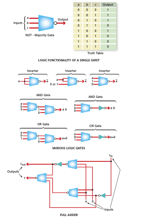
With proper choice of the specific dimensions for the gates, channels, and ancillary features of the generic G4-FET, the device could be made to function as a three-input, oneoutput logic gate. As illustrated by the truth table in the top part of the figure, the behavior of this logic gate would be the inverse (the NOT) of that of a majority gate. In other words, the device would function as a NOT-majority gate. By simply adding an inverter, one could obtain a majority gate. In contrast, to construct a majority gate in conventional complementary metal oxide/semiconductor (CMOS) circuitry, one would need four three-input AND gates and a four-input OR gate, altogether containing 32 transistors.
The middle part of the figure schematically depicts three ways of realizing an inverter (NOT gate), two ways of realizing an AND gate, and two ways of realizing an OR gate by use of one or two NOT-majority gates. In addition (not shown in the figure), by using one of the three inputs as a programming or control input that is set to 0 or 1, a NOT-majority could be made to respond to the other inputs as either a NAND or a NOR gate, respectively. Inasmuch as the sets {NOT,AND}, {NOT,OR}, and {NAND,NOR} have previously been shown to be universal (in the sense that any digital computation or logic function could be realized by use of suitable combinations of members of these sets), the possibility of realizing these sets signifies that the NOT-majority gate is also universal.
The bottom part of the figure depicts a full adder, implemented by use of three NOT-majority gates and two inverters, that would put out two one-bit binary numbers in response to three input one-bit binary numbers. The design of this adder exploits the possibility of switching a NOT-majority gate between NAND and NOR functionality to minimize the number of gates needed. In contrast, the simplest implementation of an equivalent full adder based on Boolean gates would include nine NAND gates and four inverters.
This work was done by Travis Johnson, Amir Fijany, Mohammad Mojarradi, Farrokh Vatan, Nikzad Toomarian, Elizabeth Kolawa, Sorin Cristoloveanu, and Benjamin Blalock of Caltech for NASA’s Jet Propulsion Laboratory. For more information, download the Technical Support Package (free white paper) at www.techbriefs.com/tsp under the Electronics/Computers category. In accordance with Public Law 96-517, the contractor has elected to retain title to this invention. Inquiries concerning rights for its commercial use should be addressed to:
Innovative Technology Assets Management
JPL
Mail Stop 202-233
4800 Oak Grove Drive
Pasadena, CA 91109-8099
(818) 354-2240
E-mail: This email address is being protected from spambots. You need JavaScript enabled to view it.
Refer to NPO-41698, volume and number of this NASA Tech Briefs issue, and the page number.
This Brief includes a Technical Support Package (TSP).
G4-FETs as Universal and Programmable Logic Gates
(reference NPO-41698) is currently available for download from the TSP library.
Don't have an account?
Overview
The document discusses the G4FET, a novel semiconductor device developed by NASA's Jet Propulsion Laboratory that integrates both Metal-Oxide-Semiconductor Field-Effect Transistor (MOSFET) and Junction Field-Effect Transistor (JFET) technologies within a single structure. This device is built using Silicon-On-Insulator (SOI) technology, which allows for enhanced flexibility and isolation. The G4FET features four independent gates: two side junction-based gates, a top MOS gate, and a back gate activated by the SOI substrate. This unique configuration enables precise control over the conduction characteristics of the transistor.
The G4FET operates by utilizing the body of the MOSFET as its channel, allowing it to function as both an inversion-mode p-channel MOSFET and an accumulation/depletion-mode n-channel G4FET. The document highlights the advantages of this design, including the ability to manipulate multiple gates, which is challenging in traditional bulk-CMOS technology. The G4FET's structure allows for the implementation of various logic functions, making it a universal logic gate capable of simulating any basic logic gate. It is also programmable, meaning that one of its inputs can be fixed to create specific logic functions, such as a simple full adder circuit.
The document emphasizes the potential applications of the G4FET in low-power modulation for RF applications, as well as in analog and mixed-signal circuits. The ability to independently control four gates provides exciting opportunities for circuit design, enhancing performance as technology scales down. The G4FET's design is particularly amenable to modern trends in microelectronics, as it can achieve better performance with optimized body doping and reduced gate lengths.
In summary, the G4FET represents a significant advancement in transistor technology, combining the benefits of both MOSFET and JFET into a single device. Its unique four-gate structure allows for versatile applications in various electronic circuits, paving the way for innovations in digital, analog, and RF technologies. The document serves as a technical support package, providing insights into the G4FET's structure, operation, and potential applications in the field of microelectronics.