
A proposed integrated circuit would translate (1) a pair of input signals having a low differential potential and a possibly high common-mode potential into (2) a pair of output signals having the same low differential potential and a low common-mode potential. As used here, “low” and “high” refer to potentials that are, respectively, below or above the nominal supply potential (3.3 V) at which standard complementary metal oxide/semiconductor (CMOS) integrated circuits are designed to operate. The input common-mode potential could lie between 0 and 10 V; the output common-mode potential would be 2 V. This translation would make it possible to process the pair of signals by use of standard 3.3-V CMOS analog and/or mixed-signal (analog and digital) circuitry on the same integrated-circuit chip. A schematic of the circuit is shown in the figure.
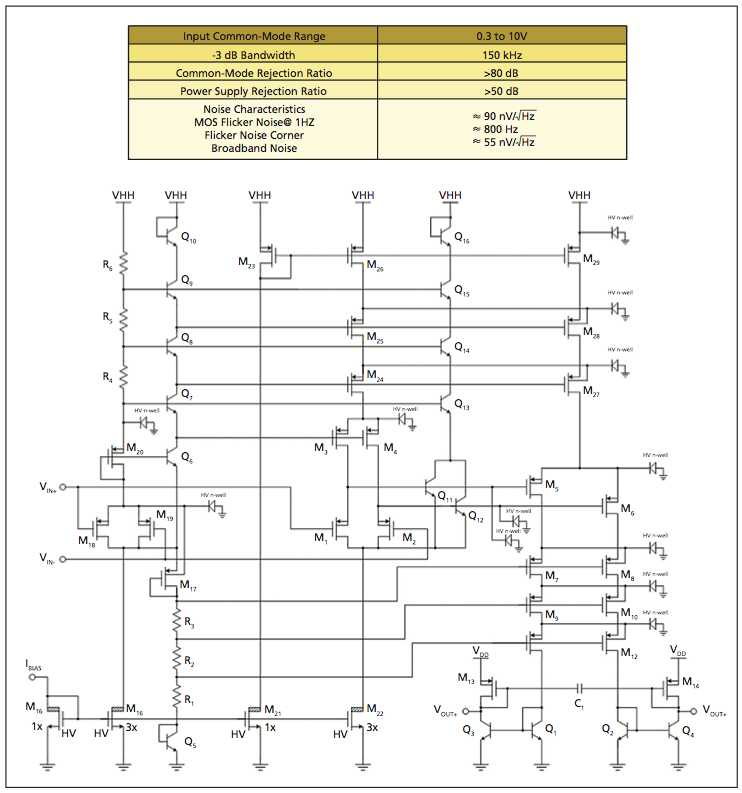
In the proposed circuit, the input signals would be coupled into both a level-shifting pair and a common-mode-sensing pair of CMOS transistors. The output of the level-shifting pair would be fed as input to a differential pair of transistors. The resulting differential current output would pass through six standoff transistors to be mirrored into an output branch by four heterojunction bipolar transistors. The mirrored differential current would be converted back to potential by a pair of diode-connected transistors, which, by virtue of being identical to the input transistors, would reproduce the input differential potential at the output.
The common-mode-sensing pair would be used to set the control potential for a biasing circuit that would provide the proper terminal potentials for protecting all devices against excessive excursions of potential for a common-mode potential range of 0 to 12 V. The biasing circuit would include high-voltage-drain transistors capable of withstanding the full high input potentials on their drains; the incorporation of these transistors would enable simplification of part of the bias circuit and of the circuitry associated with the input transistor pairs. High-voltage n-wells would enable floating of substrates of pchannel metal oxide/semiconductor field-effect transistors to potentials as high as tens of volts, whereas devices containing standard n-wells break down at potentials between 6 and 7 V, even though maximum gate-to-source and drain-to-source potentials remain at 3.3 V.
The expected performance of the circuit has been studied in computational simulations. The table presents values of some performance parameters determined from the results of the simulations.
This work was done by Jeremy A. Yager, Mohammad M. Mojarradi, and Tuan A. Vo of Caltech and Benjamin J. Blalock from University of Tenn., Knoxville for NASA’s Jet Propulsion Laboratory. NPO-45762
This Brief includes a Technical Support Package (TSP).
High-Voltage-Input Level Translator Using Standard CMOS
(reference NPO-45762) is currently available for download from the TSP library.
Don't have an account?
Overview
The document is a Technical Support Package from NASA's Jet Propulsion Laboratory (JPL) detailing the development of a High-Voltage-Input Level Translator using Standard CMOS technology. This innovation addresses the growing need for reliable voltage translation in applications such as aerospace, automotive, and medical fields, where sensing small differential voltages across a wide common-mode range is critical.
The background highlights the challenges posed by the increasing prevalence of low-voltage-only CMOS processes, which are optimized for low-power and high-speed digital and mixed-signal applications. As a result, there is a demand for medium-to-high voltage semiconductor processes that are often non-standard and specialized. The document outlines the design and functionality of a linear high-voltage level shifter, which is essential for interfacing low-voltage circuits with high-voltage environments.
Key components of the design include high-voltage (HV) Lateral Double-Diffused MOS (LDMOS) transistors and HV N-well structures. The LDMOS transistor, developed in-house at JPL, boasts a breakdown voltage exceeding 50 V, which is crucial for the operation of the circuit. The HV N-well allows PFET MOS transistors to operate with their substrates floated to voltages up to the same breakdown voltage, enhancing the circuit's performance and reliability.
The document also discusses the biasing techniques employed to manage the high voltages required for the circuit's operation. These techniques ensure that the input devices can follow the input signal from ground to 12 V while providing voltage standoff protection for the signal path. The bias circuits are designed to generate gate voltages for the standoff transistors, ensuring proper functionality across varying voltage levels.
Figures included in the document illustrate the layout of the linear level-shifting buffer and the biasing circuits, providing a visual representation of the design's architecture. The document emphasizes the importance of these developments in advancing technology that can withstand extreme environments, making it suitable for various applications beyond aerospace.
Overall, this Technical Support Package serves as a comprehensive overview of the innovative high-voltage input level translator, showcasing JPL's contributions to semiconductor technology and its potential impact on multiple industries.