
Focal-plane-array (FPA) hybrids of quantum-well infrared photodetectors (QWIPs) thinned to the membrane level are undergoing development. The developmental QWIPs in question are of the kind that exploit bound-to-quasi-bound absorption, as described, for example, in "Bound-to-Quasi-Bound Quantum-Well Infrared Photodetectors," which immediately follows this article. The present development encompasses both the thinned-array design and the method of fabrication.
Unthinned and partially thinned QWIP FPA hybrids developed previously have been characterized by crosstalk among pixels, thermal mismatches between the FPA hybrids and associated readout multiplexers, and poor light-coupling efficiency. The developmental thinned QWIP FPAs overcome these deficiencies and offer other improvements in performance, as follows:
- The thermal masses of FPAs are so small that they adapt the thermal expansion and contraction coefficients of Si CMOS (complementary metal oxide/semiconductor) readout multiplexers.
- The more favorable aspect ratios created by thinning maximize the efficiency of coupling of light from random reflectors.
- Crosstalk among pixels is suppressed because after thinning, the remaining substrate thickness is too small to support appreciable crosstalk.
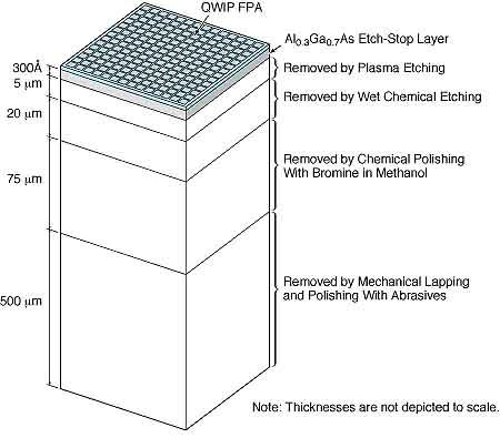
A QWIP FPA of the present type is fabricated on top of a 300-Å-thick layer of Al0.3Ga0.7As that, in turn, has been deposited on a relatively thick (several hundred µm) GaAs substrate. Then the thinned QWIP FPA is formed by removing the substrate from under the Al0.3Ga0.7As layer in the following sequence of processes:
- Formation of a QWIP FPA hybrid via indium bump-bonding process. This hybrid consists of QWIP FPA and Si CMOS readout multiplexer.
- The hybrid is backfilled with low-viscosity epoxy.
- By mechanical lapping and polishing with abrasives, most of the thickness is removed from the bottom side, leaving a substrate thickness of 100 µm.
- Chemical polishing with a solution of 1 part bromine and 100 parts methanol is used to remove the next 75 µm.
- The next 20 µm of thickness is removed in an 8-minute wet-chemical etch with a solution of 5 parts H2SO4, 40 parts H2O2, and 100 parts H2O.
- The remaining 5 µm of substrate thickness is removed by dry etching in a plasma formed from CCl2F2 gas. The Al0.3Ga0.7As layer acts as an etch-stop layer during this process, in that the plasma etches the GaAs substrate material much faster than it etches Al0.3Ga0.7As.
- An O2 plasma is used to remove a grayish film that remains after the CCl2F2 plasma etch.
This work was done by Sarath Gunapala, John K. Liu, and Mani Sundaram of Caltech for NASA's Jet Propulsion Laboratory. In accordance with Public Law 96-517, the contractor has elected to retain title to this invention. Inquiries concerning rights for its commercial use should be addressed to
Technology Reporting Office
JPL
Mail Stop 122-116
4800 Oak Grove Drive
Pasadena, CA 91109
(818) 354-2240
Refer to NPO-19833
This Brief includes a Technical Support Package (TSP).
Fabrications of thinned QWIP arrays for improved performance
(reference NPO19833) is currently available for download from the TSP library.
Don't have an account?
Overview
The document outlines a technical report from NASA's Jet Propulsion Laboratory (JPL) regarding the fabrication of thinned Quantum-Well Infrared Photodetector (QWIP) arrays aimed at improving their performance. The report highlights several key issues associated with unthinned or partially thinned focal plane array (FPA) hybrids, including pixel-to-pixel crosstalk, thermal mismatches between the focal plane array and the readout multiplexer, and poor light coupling efficiency.
To address these problems, the proposed solution involves thinning the QWIP focal plane to a membrane level. This process significantly reduces the thermal mass, thereby eliminating thermal mismatches and enhancing light coupling efficiency. The thinning process also minimizes the substrate material, which helps to stop pixel-to-pixel crosstalk due to the reduced substrate left after thinning.
The fabrication process is detailed in several steps. Initially, the sample is mechanically polished to reduce the thickness to approximately 100 micrometers. Following this, a wet-chemical etching process is employed to remove an additional 75 micrometers of the GaAs substrate using a specific solution. The final 5 micrometers of substrate thickness is removed through a selective dry etching process using plasma formed from CCl₂F₂ gas, with an Al₀.₃Ga₀.₇As layer acting as an etch-stop layer. An O₂ plasma is then used to eliminate any residual film left after the dry etching.
The report emphasizes the innovative aspects of the thinning process, particularly the use of selective dry etching, which allows for precise control over the material removal while preserving the integrity of the QWIP device structure. The overall goal of this research is to enhance the performance of QWIP arrays, leading to reduced dark current and crosstalk, ultimately improving the efficiency and effectiveness of infrared detection systems.
The document concludes with a notice regarding the rights for commercial use of the invention, indicating that inquiries should be directed to the Technology Reporting Office at JPL. The work was conducted by a team of researchers, including Sarath Gunapala, John K. Liu, and Mani Sundaram, and is part of ongoing efforts to advance infrared detection technologies for various applications.