Experiments have shown that a substrate can be patterned with submicron features by the following procedure:
- Coat the substrate with a layer of poly(methyl methacrylate) [PMMA], which will serve as an electron-beam resist to be patterned into an etch mask.
- Pattern the PMMA by electron-beam lithography.
- Ion-etch through the PMMA to transfer the pattern to the substrate.
The procedure has been used to fabricate a 600-nm-pitch diffraction grating; it could also be used to form submicron features on semiconductor and other devices.
Prior to the development of this procedure, it was known that submicron features can be produced in a PMMA resist by exposing it to an electron beam, then developing it. However, the transfer of submicron features from a PMMA mask to a substrate by either dry or wet etching had not been demonstrated. As a result of the development of the present procedure, it is now known that success in the transfer of submicron features depends on the proper choice of the substrate material(s), the thicknesses of the substrate and PMMA, the etching method, and the etching conditions.
The substrate for the 600-nm-pitch grating was a 100-nm-thick gold film on a 5-nm-thick chromium layer on a quartz disk; the Cr and Au films were deposited on the disk in an electron-beam evaporation system. A PMMA resist 120 nm thick was spun onto the Au surface.
The 600-nm-pitch grating pattern was imparted to the PMMA by use of an electron-beam lithography machine. The electron-beam dose in the exposed regions was about 200 µC/cm2, and the beam current was 5 nA. Following the electron-beam exposure, the pattern in the resist was developed by use of a 1:3 mixture of methyl isobutyl ketone and isopropyl alcohol.
The ion etching technique used to transfer the pattern to the substrate could be characterized, more precisely, as milling by a beam of argon ions. The etching was performed in an argon-ion-milling system that included an ion-beam source in a vacuum chamber that was capable of evacuation to a base pressure of 4 × 10 -8 torr (≈5 µPa). During operation of the ion-beam source, the pressure of argon in the system was raised to 2 ×10 -4 torr (≈0.03 Pa) by addition of argon gas to the chamber at a controlled rate. This operating pressure was chosen to be high enough to generate a sufficient population of ions to obtain the desired beam current density, but not so high that the beam would be excessively dispersed through collisions with gas molecules.
The ion-beam-generating potential was 1.5 kV. The total beam current was 10 mA. The beam was spread over a cross section approximately 5 cm in diameter. The etching time was about 2 minutes.
This work was done by Thomas George, Richard Muller, Paul Maker, and David Barsic of Caltech for NASA's Jet Propulsion Laboratory.
NPO-20649
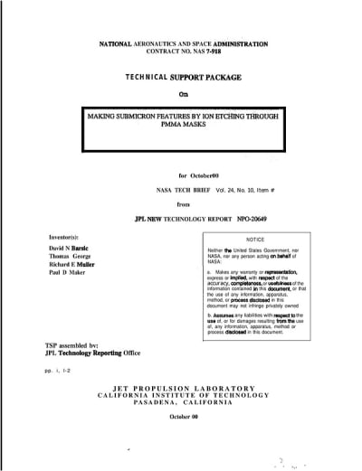
This Brief includes a Technical Support Package (TSP).

Making Submicron Features by Ion Etching Through PMMA Masks
(reference NPO20649) is currently available for download from the TSP library.
Don't have an account?
Overview
The document outlines a procedure developed for fabricating submicron features on substrates using a combination of electron-beam lithography and ion etching techniques. This method is particularly significant for creating patterns with a pitch of 600 nanometers, which can be applied to semiconductor devices and other technologies.
The process begins with the coating of a substrate with a layer of poly(methyl methacrylate) (PMMA), which acts as an electron-beam resist. The PMMA is then patterned using an electron-beam lithography machine, where an electron dose of approximately 200 μC/cm² and a beam current of 5 nA are employed. After exposure, the pattern in the PMMA is developed using a mixture of methyl isobutyl ketone and isopropyl alcohol.
To transfer the pattern from the PMMA mask to the substrate, ion etching is utilized, specifically through argon ion milling. The etching process occurs in a vacuum chamber with a base pressure of 4 × 10⁻⁸ torr, where argon gas is introduced to maintain an operational pressure of 2 × 10⁻⁴ torr. This pressure is optimized to ensure a sufficient population of ions while minimizing excessive dispersion of the ion beam. The ion-beam-generating potential is set at 1.5 kV, with a total beam current of 10 mA, and the etching time is approximately 2 minutes.
The substrate used for the 600-nm-pitch grating consists of a 100-nm-thick gold film on a 5-nm-thick chromium layer, deposited on a quartz disk. The successful transfer of submicron features is contingent upon careful selection of substrate materials, PMMA thickness, etching methods, and conditions.
The work was conducted by a team from Caltech for NASA’s Jet Propulsion Laboratory, highlighting the collaboration between academic research and governmental space exploration efforts. The document emphasizes the critical importance of material choice and process parameters in achieving successful outcomes in the fabrication of submicron features.
Overall, this innovative procedure represents a significant advancement in the field of nanofabrication, enabling the production of intricate patterns that are essential for the development of advanced electronic devices and other applications in technology.

