
An improved process for the fabrication of random arrays of silicon nanotips has been demonstrated to be feasible. Relative to other such processes, this process offers advantages of low cost and simplicity. Moreover, this process can readily be combined with other processes used to fabricate integrated circuits and other monolithic silicon structures.
Arrays of silicon nanotips are subjects of research and development efforts directed toward utilizing them as field emitters in flat-panel displays, vacuum microelectronics, and microwave devices.Other silicon-nanotip-fabrication processes developed thus far predominantly include lithography, etching, and/or elaborate deposition steps followed by oxide sharpening steps and are both process intensive as well as expensive. In addition to being cheaper and simpler, the present process can efficiently produce silicon nanotips that range in height from a few microns to several tens of microns and are distributed over large areas.
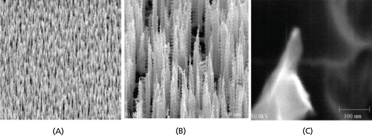
The process mentioned here can be summarized as consisting of (1) the growth of micro-etch masks on a silicon substrate, followed by (2) etching away of the masks, along with some of the substrate, to make an array of sharp tips. In the first step of the process, a cleaned silicon substrate is subjected to reactive ion etching (RIE)in a certain mixture of oxygen and carbon tetrafluoride under radio-frequency excitation. This process step results in the growth of fluorine based compounds in the form of stumps randomly distributed on the substrate. These stumps are known in the art as "polymer RIE grass." The dimensions of these stumps are of the order of hundreds of nanometers, the exact values depending on process time and gas composition. The areal density of the stumps decreases with increasing process time as they grow and merge with neighboring stumps.These stumps constitute the micro-etch masks for the next step of the process.
In the second step of the process, the substrate covered with the micro-etch masks is subjected to deep reactive ion etching (DRIE) process, which consists of cycles of reactive ion etching alternating with passivation (the Bosch process). The gas used in the etching substeps is sulfur hexafluoride (SF6); the gas used in the passivation substeps is octafluorocyclobutane (C4F8). The portions of the substrate directly under the RIE grass stubs are etched more slowly than are the portions between the stubs. Hence, what remains at the end of the process, after the stubs and parts of the substrate have been etched away, are silicon spikes where the stubs were (see figure).
In a variation of the process, one starts with a silicon or silicon-on-insulator substrate with the intent to etch through the full thickness of the substrate. That is to say, one chooses the thickness so that the DRIE step releases individual nanotips. Such individual silicon nanotips may have utility as microscopic probes in biomedical applications.
This work was done by Harish Manohara of Caltech for NASA's Jet Propulsion Laboratory. For further information, access the Technical Support Package (TSP) free on-line at www.techbriefs.com/tsp under the Manufacturing category.
In accordance with Public Law 96-517, the contractor has elected to retain title to this invention. Inquiries concerning rights for its commercial use should be addressed to:
Innovative Technology Assets Management
JPL Mail Stop 202-233
4800 Oak Grove Drive
Pasadena,CA 91109-8099
(818)354-2240
E-mail: This email address is being protected from spambots. You need JavaScript enabled to view it.
Refer to NPO-40123, volume and number of this NASA Tech Briefs issue, and the page number.
This Brief includes a Technical Support Package (TSP).
(NANO) A New Process for Fabricating Random Silicon Nanotips
(reference NPO-40123) is currently available for download from the TSP library.
Don't have an account?
Overview
The document presents a new technique developed by NASA's Jet Propulsion Laboratory (JPL) for fabricating silicon nanotips, which are of significant interest for applications in flat-panel displays, vacuum microelectronics, and microwave devices. The innovative process is characterized by its simplicity, low cost, and compatibility with existing silicon fabrication methods.
The fabrication technique involves two main steps utilizing reactive ion etching (RIE). In the first step, a cleaned silicon substrate undergoes RIE in a mixture of oxygen and carbon tetrafluoride, resulting in the formation of polymer "RIE-grass" structures. These structures serve as micro-etch masks for the subsequent deep reactive ion etching (DRIE) step, where the actual silicon nanotips are created. This method allows for the production of nanotips with heights ranging from a few microns to several tens of microns, distributed over large areas.
One of the key advantages of this new process is its inherent capability to integrate easily with monolithic silicon fabrication schemes, making it suitable for creating complex structures such as integrated extraction and multiple focusing grid systems. This is particularly beneficial compared to other nanotip fabrication methods, such as those involving carbon nanotubes or metallic nanowires, which tend to be more process-intensive.
The document emphasizes that the silicon nanotips produced can be utilized in field emission applications, either with or without coatings, enhancing their versatility. The simplicity of the process not only reduces costs but also streamlines the production of silicon nanotips, making it a promising alternative to traditional methods that rely heavily on lithography, etching, and elaborate deposition techniques.
Overall, this new technique represents a significant advancement in the field of nanotechnology, offering a more efficient and cost-effective approach to the fabrication of silicon nanotips, which could lead to broader applications in various electronic devices and systems. The work is attributed to Harish M. Manohara and is part of ongoing research efforts at JPL to explore the potential of silicon nanotips in modern technology.