
GaAs/AlxGa1-xAs quantum-well infrared photodetectors (QWIPs) with broad-band responses are undergoing development. The broad-band responses are obtained by varying the depths and widths of the wells and the thicknesses of the barriers between the wells, as explained below.
A GaAs/AlxGa1-xAs QWIP contains layers of GaAs (the wells) alternating with layers of AlxGa1-xAs (0< x <1) (the barriers). Detection of a photon in a QWIP involves photoexcitation of electrons from the ground to the first excited quantum state of one of the wells. The excited electron can escape from the well and, if a suitable bias voltage is applied, then many such photoelectrons are collected as photocurrent.
Typically, a QWIP is of the bound-to-continuum or the bound-to-quasi-bound type. In the bound-to-continuum type, the first excited state lies above the top of the well. In the bound-to-quasi-bound type, the first excited state lies exactly at the top of the well. Each of these types offers a different advantage; the spectral width of photoresponse is broader in the bound-to-continuum type, while the bound-to-quasi-bound case offers the advantage of a smaller thermionic contribution to dark current.
The height of each barrier, and thus the depth of an adjacent well, is determined by the mole fraction (x) of aluminum. The energy heights of ground and first excited states relative to the tops and bottoms of the wells, plus the spectral responses of QWIPs, are determined by the widths of the wells, the thicknesses and heights of the barriers, and the well-doping densities. These thicknesses and compositions can be chosen by design and implemented with established deposition techniques.
In a typical bound-to-quasi-bound QWIP of older design, all of the wells are of the same width and doping density, and all of the barriers are of the same thickness and the same aluminum content. The spectral width of its photoresponse is about 10 percent of its peak-response wavelength, which can be set at a value between 6 and 20 µm by suitable choice of layer thicknesses and x.
A device with broader spectral response can be constructed by stacking different quantum wells in a repeating sequence. Each sequence contains several quantum wells; the thicknesses and compositions of the barrier and well layers within each sequence can be tailored to optimize each well for a different pass band that partly overlaps one or more pass band(s) of the other wells in the sequence. The net effect of the multiple partial overlaps is a broader overall pass band for the QWIP device as a whole.
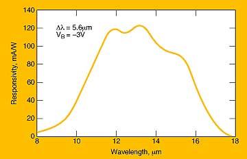
An experimental device of this type was made with 35 repeating three-well sequences. The wells in each sequence were designed for peak responses at wavelengths of 13.5, 14.3, and 15.5 µm, respectively. The measured spectral response of this device (see figure) was found to be about 4 times as broad as that of a typical bound-to-quasi-bound QWIP of older design for the same nominal peak wavelength
This work was done by Sumith Bandara and Sarath Gunapala of Caltech for NASA's Jet Propulsion Laboratory. For further information, access the Technical Support Package (TSP) free on-line at www.techbriefs.com under the Electronic Components and Systems category. In accordance with Public Law 96-517, the contractor has elected to retain title to this invention. Inquiries concerning rights for its commercial use should be addressed to
Technology Reporting Office JPL Mail Stop 122-116 4800 Oak Grove Drive Pasadena, CA 91109 (818) 354-2240
Refer to NPO-20319, volume and number of this NASA Tech Briefs issue, and the page number.
This Brief includes a Technical Support Package (TSP).
Broad-Band GaAs/AlxGa1-xAs QWIPs
(reference NPO-20319) is currently available for download from the TSP library.
Don't have an account?
Overview
The document provides details about two significant engineering and technology expos scheduled for September and November 1999.
The first event is the New England Design & Manufacturing Expo, taking place from September 20-22, 1999, at the Hynes Convention Center in Boston, MA. This expo focuses on the latest products and services designed to assist engineers in overcoming challenges related to design, prototyping, testing, and production. A highlight of the event is the CAD & Rapid Prototyping Pavilion, which showcases advancements in computer-aided design and rapid prototyping technologies. The expo is colocated with two other notable events: Photonics East, which is the only optics and photonics exhibition in the Northeast, and Electronic Imaging International, recognized as the East Coast’s premier annual imaging expo.
The second event, Technology 2009, is scheduled for November 1-3, 1999, at the Fontainebleau Hilton in Miami Beach, Florida. This is the tenth annual "Engineering Innovation Show," which serves as a major platform for showcasing new and next-generation technologies available for licensing and commercial development. It is colocated with the Southeast Design & Manufacturing Expo, which specifically targets the high-tech corridor in the Southeast, and the Small Business Tech Expo, which is focused on resources and technologies for launching new products and fostering partnerships.
Both expos promise to be valuable opportunities for attendees to explore cutting-edge engineering solutions, gain insights into product and business ideas, and establish profitable partnerships. The document encourages potential attendees to plan their visit and highlights that hundreds of exhibits will be available for free. For further information, attendees are directed to contact specific representatives or visit the provided website.
Overall, these events are positioned as essential gatherings for professionals in the engineering and technology sectors, offering a comprehensive look at innovations and resources that can drive future developments in the industry.