
Quantum-well infrared photodetectors (QWIPs) that are designed to exploit transitions between bound and quasi-bound electron quantum states and that incorporate random reflectors are undergoing development. Focal-plane arrays of such detectors are also undergoing development, all as part of a continuing effort to increase the responsivities and decrease the noise levels (dark currents) of infrared-imaging devices operating at wavelengths from about 3 to about 18 µ.
QWIPs have been discussed in numerous prior articles in NASA Tech Briefs. Two articles with particular relevance to the present devices were "Bound-to-Quasi-Bound Quantum-Well Infrared Photodetectors" (NPO-19633), Vol. 22, No. 9 (September 1998), page 54 and "Demonstration of 15 µ 128 x 128 Quantum Well IR Photodetector Imaging Camera" (NPO-19407) Vol. 20, No. 11 (November 1996), page 30. The first-mentioned article discussed, in some detail, the advantage of designing QWIPs to exploit bound-to-quasi-bound transitions to reduce dark currents below those achievable in QWIPs that exploit bound-to-continuum transitions. The second-mentioned article included a passing mention of the use of random reflectors to increase the efficiency of coupling of light into the QWIPs. In the time since the second-mentioned article, more information on the random reflectors has become available, and is presented below.
The light-coupling problem was discussed in yet another prior article; namely, "Cross-Grating Coupling for Focal-Plane Arrays of QWIPs" (NPO-19657), NASA Tech Briefs, Vol. 22, No. 1 (January 1998), page 6a. To recapitulate: (1) The direction through the thicknesses of the quantum wells is parallel to the focal plane; (2) Quantum selection rules allow the detection of only that part of the incident light that is electrically polarized along the direction through the thicknesses of the quantum wells and thus perpendicular to the focal plane; and (3) The light to be detected is incident along directions approximately perpendicular to the focal plane, and thus only a small fraction of it is electrically polarized along the thicknesses of the quantum wells. Prior to the development of the random reflectors, light-coupling efficiency was increased by illuminating QWIPs via facets inclined 45° to the directions through the thicknesses of their quantum wells. However, the 45° coupling scheme is not suitable for two-dimensional imaging arrays of QWIPs. The random-reflector scheme is suitable for two-dimensional arrays.
Many more passes of infrared light inside a QWIP, with a corresponding increase in responsivity over that achievable with a 45° facet, can be obtained by incorporating a randomly roughened reflecting surface on top of the QWIP. The random structure of the reflector prevents the light from being diffracted perpendicularly backward after the second bounce, as happens in the case of a cross-grating coupling like that discussed in the third-mentioned prior article. After each bounce, light is scattered at a different random angle, and the only chance for light to escape from the detector occurs when it is reflected toward the surface within the critical angle of the perpendicular. For a GaAs/air interface, this angle is about 17°, defining a very narrow escape cone for the trapped light.
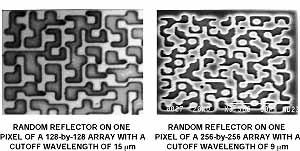
The QWIP in each pixel of an array according to the present design concept contains a random reflector (see figure) with scattering surfaces at two levels separated by a quarter of the wavelength of interest in GaAs. The area of the top (unetched) level equals the area of the bottom (etched) level. The combination of equal areas and quarter-wavelength separation maximizes the destructive interference of light reflected from the two levels along the perpendicular, thus limiting the leakage of light through the escape cone. This random reflector structure can be fabricated by use of standard photolithography and selective dry etching with CCl2F2. The advantage of photolithography over a completely random fabrication process is the ability to accurately control the sizes of features to preserve pixel-to-pixel uniformity.
This work was done by Sarath Gunapala, John K. Liu, Mani Sundaram, and Jin S. Park of Caltech for NASA's Jet Propulsion Laboratory. In accordance with Public Law 96-517, the contractor has elected to retain title to this invention. Inquiries concerning rights for its commercial use should be addressed to
Technology Reporting Office
JPL
Mail Stop 122-116
4800 Oak Grove Drive
Pasadena, CA 91109
(818) 354-2240
Refer to NPO-19815
This Brief includes a Technical Support Package (TSP).
Bound-to-quasi-bound QWIPs with random reflectors
(reference NPO19815) is currently available for download from the TSP library.
Don't have an account?
Overview
The document is a New Technology Report from the Jet Propulsion Laboratory (JPL) detailing advancements in long-wavelength infrared (LWIR) quantum well infrared photodetectors (QWIPs) with a focus on a specific case, NPO-19815. The report outlines a novel device and method for a GaAs/AlGaAs Focal Plane Array (FPA) designed to operate within the 6 to 18 µm infrared wavelength range. This technology represents an improvement over previous models, specifically NPO 19407/9009, which featured a 15μm cutoff 125x125 GaAs QWIP FPA camera.
The key innovation in this report is the incorporation of a random reflector that enhances light coupling efficiency to the photodetector. This design aims to improve the sensitivity and performance of infrared detection, making it suitable for various space applications. These applications include monitoring global atmospheric temperature profiles, assessing relative humidity, analyzing cloud characteristics, detecting minor atmospheric constituents, and identifying cold objects such as ballistic missiles during their midcourse phase.
The report also discusses the technical aspects of the QWIP, including the concept of bound-to-quasi-bound transitions, which involve a thermionic emission energy barrier that is precisely tuned for optimal performance. The document emphasizes the potential of this technology to significantly advance infrared imaging capabilities, particularly in the context of space exploration and atmospheric studies.
The inventors of this technology are Sarath D. Gunapala, John K. Liu, Jin S. Park, and Mani Sundaram, and the report is part of a broader effort by NASA to develop advanced microelectronics for space applications. The document includes a disclaimer stating that neither the U.S. Government nor NASA guarantees the accuracy or completeness of the information provided, nor do they assume liability for any damages resulting from its use.
Overall, this report highlights a significant step forward in infrared detection technology, showcasing JPL's commitment to innovation in space science and technology, with implications for both scientific research and national security.