
A process for the fabrication of a polycrystalline diamond membrane involves chemical vapor deposition (CVD) of diamond onto a silicon substrate, followed by conventional photolithography and subsequent reactive-ion etching to remove part of the substrate (see figure). This process is an improvement over an older process in which the substrate is etched in a hot KOH solution. This process can be used to fabricate diamond polycrystalline membranes as parts of microelectromechanical sensors.
The starting substrate is a mirror-smooth (100)-oriented single-crystal silicon wafer with n or p doping to a resistivity <20 Ω·cm. To increase the density of nucleation sites for diamond and thereby make it possible to obtain a pinhole-free diamond deposit, the front (top in the figure) surface of the substrate is scratched by use of diamond paste. A polycrystalline diamond film is grown on the scratched surface by CVD from a flowing mixture or methane and hydrogen, typically at a total pressure of 45 torr (6 kPa) and a substrate temperature of 950 °C.
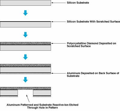
After deposition of diamond to the required thickness, aluminum is deposited on the back (bottom in the figure) surface of the substrate by electron-beam evaporation. The aluminum film is patterned photolithographically, then etched by a commercial solution containing phosphoric and acetic acids, thereby forming a mask to define the areas to be protected from, and exposed to, reactive ion etching. Next, reactive-ion etching is effected by use of a radio-frequency-induced SF6 plasma.
In an experiment, the rate of reactive-ion etching was found to be about 3.6 µm per minute; in contrast, the rate of etching in hot KOH is about 1 µm per minute. It was also found that reactive-ion etching undercut the masked portion of the substrate at a rate of about 3.5 µm per minute. The diamond membrane exposed by etching of the substrate was found to be in a state of compressive stress.
This work was done by Rajeshuni Ramesham of Caltech for NASA's Jet Propulsion Laboratory. NPO-20477
This Brief includes a Technical Support Package (TSP).
Fabricating diamond membranes using reactive-ion etching
(reference NPO20477) is currently available for download from the TSP library.
Don't have an account?
Overview
The document is a technical support package from NASA detailing a novel method for fabricating diamond membranes using reactive-ion etching, developed at the Jet Propulsion Laboratory (JPL) in collaboration with the California Institute of Technology. The research was supported by NASA's Office of Safety and Mission Assurance and acknowledges contributions from undergraduate students at Auburn University.
The primary focus of the document is on the innovative process that combines conventional photolithography with reactive ion etching to create diamond membranes suitable for microelectromechanical systems (MEMS). These diamond membranes can be utilized in various applications, including sensors and other microstructures, due to their unique properties such as high thermal conductivity, chemical stability, and mechanical strength.
The document outlines the process flow for fabricating these diamond structures, emphasizing the selective deposition of polycrystalline diamond on silicon substrates. This method allows for the creation of various microstructures, including cantilever beams and bridges, which can be supported on one or both sides, enhancing their functionality in MEMS applications.
Additionally, the document includes a disclaimer stating that neither the United States Government nor NASA makes any warranties regarding the accuracy or completeness of the information provided, nor do they assume liability for any damages resulting from its use. This is a standard precaution in technical reports to protect the organizations involved.
The report also highlights the novelty of the work, indicating that the developed process represents a significant improvement over prior methods for diamond membrane fabrication. The combination of techniques used in this research is expected to lead to advancements in the performance and reliability of MEMS devices.
Overall, this document serves as a technical brief on the advancements in diamond membrane fabrication, showcasing the potential for these materials in future technological applications. It reflects the ongoing efforts of NASA and JPL to push the boundaries of materials science and engineering, contributing to the development of innovative solutions in aerospace and other fields.