
A data-processor architecture that would incorporate elements of both conventional very-large-scale integrated (VLSI) circuitry and quantum- dot cellular automata (QCA) has been proposed to enable the highly parallel and systolic computation of fast Fourier transforms (FFTs). The proposed circuit would complement the QCA- based circuits described in several prior NASA Tech Briefs articles, namely "Implementing Permutation Matrices by Use of Quantum Dots" (NPO-20801), Vol. 25, No. 10 (October 2001), page 42; "Compact Interconnection Networks Based on Quantum Dots" (NPO-20855) Vol. 27, No. 1 (January 2003), page 32; and "Bit-Serial Adder Based on Quantum Dots" (NPO-20869), Vol. 27, No. 1 (January 2003), page 35.
The cited prior articles described the limitations of very-large-scale integrated (VLSI) circuitry and the major potential advantage afforded by QCA. To recapitulate: In a VLSI circuit, signal paths that are required not to interact with each other must not cross in the same plane. In contrast, for reasons too complex to describe in the limited space available for this article, suitably designed and operated QCA-based signal paths that are required not to interact with each other can nevertheless be allowed to cross each other in the same plane without adverse effect. In principle, this characteristic could be exploited to design compact, coplanar, simple (relative to VLSI) QCA-based networks to implement complex, advanced interconnection schemes.

To enable a meaningful description of the proposed FFT-processor architecture, it is necessary to further recapitulate the description of a quantum-dot cellular automaton from the first-mentioned prior article: A quantum-dot cellular automaton contains four quantum dots positioned at or between the corners of a square cell. The cell contains two extra mobile electrons that can tunnel (in the quantum-mechanical sense) between neighboring dots within the cell. The Coulomb repulsion between the two electrons tends to make them occupy antipodal dots in the cell. For an isolated cell, there are two energetically equivalent arrangements (denoted polarization states) of the extra electrons.
The cell polarization is used to encode binary information. Because the polarization of a nonisolated cell depends on Coulomb-repulsion interactions with neighboring cells, universal logic gates and binary wires could be constructed, in principle, by arraying QCA of suitable design in suitable patterns.

Again, for reasons too complex to describe here, in order to ensure accuracy and timeliness of the output of a QCA array, it is necessary to resort to an adiabatic switching scheme in which the QCA array is divided into subarrays, each controlled by a different phase of a multiphase clock signal. In this scheme, each subarray is given time to perform its computation, then its state is frozen by raising its interdot potential barriers and its output is fed as the input to the successor subarray. The successor subarray is kept in an unpolarized state so it does not influence the calculation of preceding subarray. Such a clocking scheme is consistent with pipeline computation in the sense that each different subarray can perform a different part of an overall computation. In other words, QCA arrays are inherently suitable for pipeline and, moreover, systolic computations. This sequential or pipeline aspect of QCA would be utilized in the proposed FFT-processor architecture.
Heretofore, the main obstacle to designing VLSI circuits for systolic and highly parallel computation of FFTs (and of other fast transforms commonly used in the processing of images and signals) has been the need for complex data permutations that cannot be implemented without crossing of signal paths. The proposed hybrid VLSI/QCA FFT-processor architecture would exploit the coplanar- signal-path-crossing capability of QCA to implement the various permutations directly in patterns of binary wires (that is, linear arrays of quantum dots), as in the example of Figure 1. The proposed architecture is based on a reformulation of the FFT by use of a particular matrix factorization that is suitable for systolic implementation. The reformulated FFT is given by
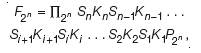
where n is an integer; F2n is a radix-2 FFT for a 2n-dimensional vector; Π2n, Si(where i is an integer), and P2n are various permutation operators or matrices; and the Ki are arithmetic operators.
Figure 2 depicts the proposed architecture. The permutation operators would be implemented by QCA modules, while the arithmetic operators Ki would be implemented by VLSI modules containing simple bit-serial processing elements. Each processing element would receive input data from two sources and would produce two outputs by performing simple multiplication and addition operations. Aside from being driven by the same clock (in order to obtain the necessary global synchronization), the processing elements would operate independently of each other; because of this feature, the processing modules would be amenable to large-scale implementation in complementary metal oxide/semiconductor (CMOS) VLSI circuitry. To obtain the necessary global synchronization, the VLSI and the QCA modules would be driven by the same clock.
This work was done by Amir Fijany, Nikzad Toomarian, Katayoon Modarres, and Matthew Spotnitz of Caltech for NASA's Jet Propulsion Laboratory. For further information, access the Technical Support Package (TSP) free on-line at www.techbriefs.com/tsp under the Computers/Electronics category. NPO-20923.
This Brief includes a Technical Support Package (TSP).
Hybrid VLSI/QCA Archetiecture for Computing FFTs
(reference NPO-20923) is currently available for download from the TSP library.
Don't have an account?
Overview
The document discusses a proposed hybrid architecture that integrates very-large-scale integrated (VLSI) circuitry with quantum-dot cellular automata (QCA) to facilitate the highly parallel and systolic computation of fast Fourier transforms (FFTs). This architecture aims to overcome the limitations of traditional VLSI circuits, particularly in handling complex data permutations required for efficient signal processing.
QCA technology is highlighted for its unique ability to allow signal paths to cross in the same plane without adverse effects, a significant advantage over VLSI, where such crossings can lead to signal interference. This characteristic enables the design of compact and coplanar QCA-based networks, which can implement advanced interconnection schemes necessary for complex computations.
The document outlines the operational principles of QCA, where each cell consists of four quantum dots and two mobile electrons that can tunnel between these dots. The polarization states of the electrons encode binary information, allowing for the construction of universal logic gates and binary wires through suitable arrangements of QCA cells. This design is particularly suitable for pipeline and systolic computations, as different subarrays can perform distinct parts of an overall computation sequentially.
The proposed architecture is expected to simplify the implementation of data permutations, which have historically posed challenges in VLSI designs for FFTs and other fast transforms used in image and signal processing. By leveraging the strengths of both VLSI and QCA, the architecture aims to enhance computational efficiency and reduce complexity.
The document also references prior NASA Tech Briefs that discuss the limitations of VLSI and the potential advantages of QCA, emphasizing the need for innovative solutions in the field of high-performance computing. The proposed hybrid architecture represents a significant step forward in the quest for efficient and powerful computational methods, particularly in applications requiring high levels of parallelism and speed.
In summary, this document presents a forward-looking approach to computing FFTs by combining VLSI and QCA technologies, aiming to address existing challenges in data processing and enhance the capabilities of future computational systems.