34,35
-1
120
30
Briefs: Sensors/Data Acquisition
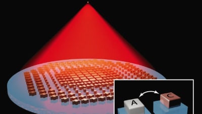
A novel nanostructure produces uniquely shaped light.
Briefs: Imaging
A wavelength of visible light is about 1,000 times larger than an electron, so the way the two affect each other is limited by that disparity. Now, researchers have come up with a way to make...

Briefs: Communications
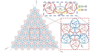
3D nanometer-scale metamaterial structures hold promise for advanced optical isolators.

Briefs: Robotics, Automation & Control
Inspired by the human finger, MIT researchers have developed a robotic hand that uses high-resolution touch sensing to accurately identify an object after grasping it just one time.
Briefs: Sensors/Data Acquisition
The "AOM" performs complex observations with ten observation modes and 175 strategies.

Briefs: Imaging
Researchers are tapping into dynamically controlled LEDs to create a simple illumination system for 3D imaging.
Briefs: AR/AI
Scientists used a novel analysis technique — called coherent correlation imaging (CCI) — to image the evolution of magnetic domains in time and space without any previous knowledge.

Briefs: Photonics/Optics
Using a new fabrication method, researchers developed a single-lens telescope and captured clear images of the lunar surface — achieving greater resolution of objects and much farther imaging distance than previous metalenses.
Briefs: Manufacturing & Prototyping
Computing using light can potentially provide lower latency and reduced power consumption, benefiting from the parallelism of optical systems.

Briefs: RF & Microwave Electronics
The ability to control light using a semiconductor device could allow low-power, relatively inexpensive sources like LEDs or flashlight bulbs to replace more powerful laser beams in new technologies.

Briefs: Photonics/Optics
The future of electronics will be based instead on using laser light to control electrical signals, opening the door for the establishment of “optical transistors” and the development of ultrafast optical electronics.
Briefs: Imaging
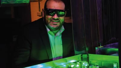
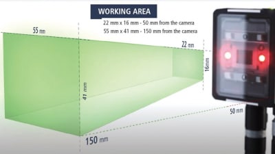
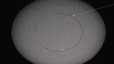
Vision sensing systems are needed to improve operations in many industrial applications, where they can be arranged to detect the presence, position, and other characteristics of objects and products.
Briefs: Test & Measurement
Engineers have developed a modeling and manufacturing technique that generates unique verification tools which simulate cracks in metals within X-ray setup part-testing geometries.
Briefs: Photonics/Optics
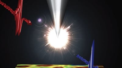
New research suggests that laser-based devices are poised to become a lot smaller.

Briefs: Photonics/Optics
Optical Signals can be retrieved from inherent background noise using Talbot effect to amplify them.
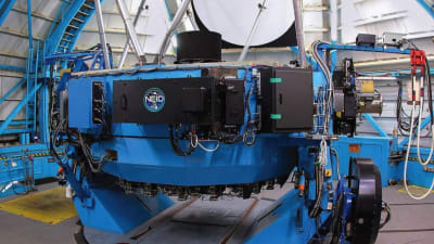
Briefs: Imaging
NASA's NEID tool delivered its first batch of data on the nearest and best-studied star, our Sun.
Briefs: Nanotechnology
3D nanometer-scale metamaterial structures hold promise for advanced optical isolators.

Briefs: Photonics/Optics
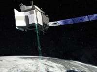
NASA’s Langley Research Center has developed a Beam Crossing Optical System for use in two-point Focused Laser Differential Interferometers.
Briefs: Sensors/Data Acquisition
A team at Johannes Gutenberg University Mainz has recently been assessing the potential for using a small, portable observation drone in remote regions.

Briefs: Photonics/Optics
The technology has several applications including optical communications, remote sensing/LiDAR, and beam steering.

Briefs: Robotics, Automation & Control
Research reveals that expertly timed lasers shined at an approaching LIDAR system can create a blind spot in front of the vehicle.

Briefs: Electronics & Computers
2D materials can be packed together more densely than conventional materials, so they could be used to make devices that run faster and perform better.
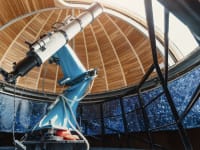
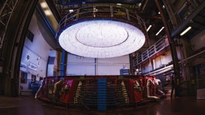
Briefs: Imaging
Nearly 20 tons of extremely pure borosilicate glass made by Ohara Corporation in Japan are becoming a honeycomb mirror measuring 27.6 feet across.
Briefs: Materials
The design may enable miniature zoom lenses for drones, cellphones, or night-vision goggles.
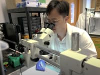
Briefs: Imaging
Scientists have developed a new characterization tool that allowed them to gain unique insight into a possible alternative material for solar cells.
Briefs: Photonics/Optics
When measuring with light, the lateral extent of the structures that can be resolved by an optical imaging system is fundamentally diffraction limited.

Briefs: Photonics/Optics
This technology will pave the way for new applications of integrated semiconductor lasers in LiDAR.
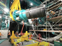
Briefs: Manufacturing & Prototyping
Researchers report that automated high-resolution electron imaging can capture the nanoscale deformation events that lead to metal failure and breakage.

Briefs: Test & Measurement
The device is 100 percent electrically controllable regarding the colors of light it absorbs, which gives it massive potential for widespread usability.

Top Stories
 Blog: Lighting
A Stretchable OLED that Can Maintain Most of Its Luminescence
 News: Energy
 INSIDER: Energy
Advancing All-Solid-State Batteries
 Blog: Energy
My Opinion: We Need More Power Soon — Is Nuclear the Answer?
 Blog: Robotics, Automation & Control
Aerial Microrobots That Can Match a Bumblebee's Speed
 Blog: Communications
Microscopic Swimming Machines that Can Sense, Respond to Surroundings
Webcasts
 Upcoming Webinars: Automotive
Advantages of Smart Power Distribution Unit Design for Automotive...
 Upcoming Webinars: Automotive
Quiet, Please: NVH Improvement Opportunities in the Early Design...
 Upcoming Webinars: Test & Measurement
From Spreadsheets to Insights: Fast Data Analysis Without Complex...
 Upcoming Webinars: Aerospace
Cooling a New Generation of Aerospace and Defense Embedded...
 Upcoming Webinars: Software
Beyond AI-Copy-Paste Engineering: Advanced AI-Integration Success...