
Efforts are underway to develop an electron-tunneling magnetometer with a "planarized" (as explained below) design. Older designs of electron-tunneling magnetometers are more three-dimensional in character and, as such, entail some difficulties of fabrication. [Such an older design was described in "Electron-Tunneling Magnetometer" (NPO-18493) NASA Tech Briefs, Vol. 17, No. 9 (September 1993), page 32.] Relative to the older designs, the present design offers advantages of sensitivity, manufacturability, and cost.
Like other tunneling-based microelectromechanical sensors, the developmental electron-tunneling magnetometer includes an electron-tunneling force/displacement transducer, wherein electrostatic-force feedback is used to counteract a force applied to a flexible cantilever or membrane by the phenomenon that one seeks to measure. The objective in the feedback scheme in any such sensor is to maintain, as closely as possible to a prescribed value, the small distance between (a) a stationary tunneling tip and (b) a counterelectrode on the cantilever or membrane. The electrostatic-deflection voltage applied to maintain the prescribed gap bears a known proportionality to the force applied to the transducer by the phenomenon that one seeks to measure. In the case of an electron-tunneling magnetometer, one seeks to measure a magnetic field through the Lorentz force that the field exerts on a known electric current in a coil of wire attached to the cantilever or membrane.
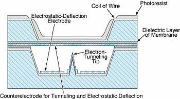
A typical electron-tunneling magnetometer of older design is fabricated from two silicon wafers. One wafer is bulk-micromachined to form the tunneling tip in a base structure; the other wafer is bulk-micromachined to form a membrane about 0.5 µm thick, at the bottom of a well about 200 µm deep (see Figure 1). The wafers are then manually assembled (membrane wafer on top, tunneling-tip wafer below) and bonded together with epoxy. The difficulties associated with the older design arise principally in connection with fabrication of the coil of wire on the relatively thin membrane at the bottom of the relatively deep well. The fabrication difficulties lead to defects and thus to poor device yield and increased costs. In addition, the membrane-in-a-well configuration limits the achievable sensitivity.
In the present version, the design and fabrication of the lower wafer are substantially the same as in the older design. However, the design of the upper wafer is different, the method of bonding the wafers is different, and most of the fabrication of the membrane in the upper wafer is deferred until after the wafers have been bonded together (see Figure 2). Prior to bonding, the faying surfaces of the two wafers (the lower surface of the upper wafer and the upper surface of the lower wafer) are coated with gold. The gold coat on the lower surface of the upper wafer is destined to become the electrode layer on the membrane; a window is formed in this coat to facilitate subsequent electrical contact with the tunneling tip and the lower electrostatic-deflection electrode.

The coated wafers are aligned, then bonded using a metal/metal thermocompression technique. Unlike in the older design, the membrane is not formed at the bottom of a well in the upper wafer. Instead, the entire upper surface of the upper wafer is etched back toward the gold layer to form the membrane, leaving a planar upper surface. Therefore, unlike in the older design, it is not necessary to manually align a recessed membrane on an upper wafer with a tunneling electrode on a lower wafer; as a result, manufacturability is enhanced and the cost of manufacture reduced. A fine coil of wire can be fabricated on top of the planar upper surface by use of conventional photoresist spin processing, more easily and with higher yield than in the case of a recessed membrane. The cost of manufacture is thus reduced further.
By enhancing manufacturability, yield, and robustness, the planarized design offers additional margin for optimization of design to increase sensitivity. As a result, the noise-floor is projected to reach 10 nT/Hz½, as compared with about 7 µT/Hz½ in the older design.
This work was done by Linda Miller, Judith Podosek, and Indrani Chakraborty of Caltech for NASA's Jet Propulsion Laboratory.
This Brief includes a Technical Support Package (TSP).
Improved electron-tunneling magnetometer
(reference NPO20317) is currently available for download from the TSP library.
Don't have an account?
Overview
The document presents a technical report on the development of an improved electron-tunneling magnetometer by the Jet Propulsion Laboratory (JPL) under NASA. This new magnetometer represents a significant advancement over previous designs, which were bulk micromachined from two silicon wafers and required complex hand-assembly processes. The innovative approach described in the report utilizes metal-to-metal thermo-pressure wafer bonding and etch-back techniques to create a monolithic, planar device. This design enhances the precision and reproducibility of the tunneling tip and control electrode's distance from the gold-coated tunneling membrane.
The report outlines the operational principles of the tunneling magnetometer, which relies on quantum mechanical tunneling of electrons across a small air gap barrier. When a voltage is applied to the electrostatic actuator, it deflects a flexible membrane, reducing the gap between the tunneling tip and the membrane to less than 50 nanometers, allowing for electron tunneling to occur. This mechanism is crucial for the magnetometer's ability to measure magnetic fields with high sensitivity.
The document also includes schematic representations of the device's design and operational components, illustrating the cross-sectional view of the prototypes and the arrangement of the electrostatic actuator and tunneling tip. The report emphasizes the advantages of the new design, including improved manufacturability and reduced costs, which are essential for practical applications in various fields, including space exploration and scientific research.
Overall, the improved electron-tunneling magnetometer showcases JPL's commitment to advancing sensor technology, providing a more efficient and effective tool for measuring magnetic fields. The report serves as a technical support package, detailing the innovations and methodologies employed in the development of this cutting-edge device, and highlights the collaborative efforts of the inventors involved in the project. This advancement not only enhances the capabilities of magnetometers but also contributes to the broader field of microelectromechanical systems (MEMS) technology.