
According to a proposal, a silicon dioxide layer in a high speed, low power, silicon-based electro-optical modulator would be replaced by a layer of lead zirconate titanate or other ferroelectric oxide material. The purpose of this modification is to enhance the power performance and functionality of the modulator.
In its unmodified form, the particular silicon-based electro-optical modulator is of an advanced design that overcomes the speed limitation of prior silicon-based electro- optical modulators. Whereas modulation frequencies of such devices had been limited to about 20 MHz, this modulator can operate at modulation frequencies as high as 1 GHz. This modulator can be characterized as a silicon-waveguide-based metal oxide/semiconductor (MOS) capacitor phase shifter in which modulation of the index of refraction in silicon is obtained by exploiting the free-charge-carrier-plasma dispersion effect. As shown in the figure, the modulator includes an n-doped crystalline silicon slab (the silicon layer of a silicon- on-insulator wafer) and a p-doped polycrystalline silicon rib with a gate oxide layer (the aforementioned silicon dioxide layer) sandwiched between them.
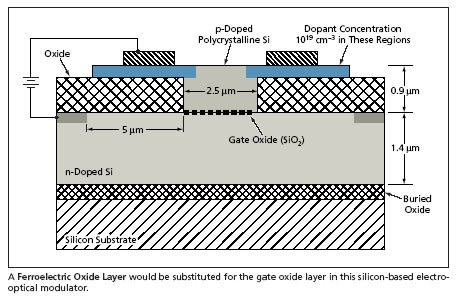 Under accumulation conditions, the majority charge carriers in the silicon waveguide modify the index of refraction so that a phase shift is induced in the optical mode propagating in the waveguide. The advantage of using an MOS capacitor phase shifter is that it is possible to achieve high modulation speed because there are no slow carrier-generation or -recombination processes involved in the accumulation operation.
The main advantage of the proposed substitution of a ferroelectric oxide layer for the silicon dioxide layer would arise from the spontaneous polarization effect of the ferroelectric layer: This spontaneous polarization would maintain accumulation conditions in the absence of applied voltage. Consequently, once the device had been switched to a given optical state, it would remain in that state, even in the absence of applied voltage (in other words, even with power turned off). A secondary advantage is that because the ferroelectric layer would have an index of refraction larger than that of silicon dioxide, there could be some reduction of optical losses attributable to fabrication of the modulator.
This work was done by Douglas Sheldon of Caltech for NASA's Jet Propulsion Laboratory. For further information, access the Technical Support Package (TSP) free online at www.techbriefs.com/tsp under the Semiconductors & ICs category.
In accordance with Public Law 96-517, the contractor has elected to retain title to this invention. Inquiries concerning rights for its commercial use should be addressed to:
Innovative Technology Assets Management
JPL
Mail Stop 202-233
4800 Oak Grove Drive Pasadena
CA 91109-8099
(818) 354-2240
E-mail: This email address is being protected from spambots. You need JavaScript enabled to view it.
Refer to NPO-40935, volume and number of this NASA Tech Briefs issue, and the page number.
This Brief includes a Technical Support Package (TSP).
Silicon-Based Optical Modulator with Ferroelectric Layer
(reference NPO-40935) is currently available for download from the TSP library.
Don't have an account?
Overview
The document discusses a recent advancement in silicon-based optical modulators, specifically focusing on a design that incorporates a ferroelectric layer, such as lead-zirconate-titinate (PZT), to enhance performance. Traditional silicon optical modulators have faced limitations, particularly in modulation speed, with previous designs achieving only around 20 MHz. The new design addresses this issue by utilizing the free carrier plasma dispersion effect, allowing for modulation frequencies to reach up to 1 GHz.
The operation of the modulator is based on the accumulation of majority carriers in the silicon waveguide, which modifies the refractive index and induces a phase shift in the optical mode. A key advantage of this design is the use of a metal-oxide-semiconductor (MOS) capacitor phase shifter, which eliminates slow carrier generation and recombination processes, thus enabling high modulation speeds.
One of the significant innovations presented in this document is the replacement of the silicon dioxide layer, traditionally used as a gate oxide, with a ferroelectric layer. This change is beneficial because ferroelectric materials can maintain polarization conditions even without an applied voltage, reducing the power required to keep the device in a switched position. Once the device is activated, power can be removed, leading to energy efficiency.
Additionally, the ferroelectric layer has a higher index of refraction compared to silicon dioxide, which may help reduce potential loss mechanisms during device manufacturing. This improvement could enhance the overall performance and efficiency of silicon-based photonic devices.
The document is part of a Technical Support Package from NASA's Jet Propulsion Laboratory, aimed at disseminating aerospace-related technological advancements with broader scientific and commercial applications. It emphasizes the potential of this new optical modulator design to contribute to the field of photonics, particularly in applications requiring high-speed data transmission and processing.
Overall, the integration of ferroelectric materials into silicon optical modulators represents a significant step forward in overcoming the limitations of traditional silicon photonics, paving the way for faster and more efficient optical communication technologies.