
To increase the usefulness of monolithic millimeter-wave integrated circuit (MMIC) components at submillimeter-wave frequencies, a chip has been designed that incorporates two integrated, radial E-plane probes with an MMIC amplifier in between, thus creating a fully integrated waveguide module. The integrated amplifier chip has been fabricated in 35-nm gate length InP high-electron-mobility-transistor (HEMT) technology. The radial probes were mated to grounded coplanar waveguide input and output lines in the internal amplifier. The total length of the internal HEMT amplifier is 550 μm, while the total integrated chip length is 1,085 μm. The chip thickness is 50 μm with the chip width being 320 μm.
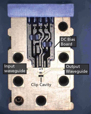
The S-parameters of the module, not corrected for input or output waveguide loss, are measured at the waveguide flange edges. The amplifier module has over 10 dB of gain from 290 to 330 GHz, with a peak gain of over 14 dB at 307 GHz. The WR2.2 waveguide cutoff is again observed at 268 GHz. The module is biased at a drain current of 27 mA, a drain voltage of 1.24 V, and a gate voltage of +0.21 V. Return loss of the module is very good between 5 to 25 dB. This result illustrates the usefulness of the integrated radial probe transition, and the wide (over 10-percent) bandwidth that one can expect for amplifier modules with integrated radial probes in the submillimeter-regime (>300 GHz).
This technology was developed for a submillimeter-wave imaging system under the DARPA SWIFT program, in collaboration with Northrop Grumman Corporation. Submillimeter-wave imaging has many applications to homeland security, hidden weapons detection, airport security, detection of bio-weapons, as well as potential applications in commercial test equipment. This technology is partially a semiconductor chip product and partially a waveguide module. The semiconductor is not fixed in its final form, but the module is essentially fixed in its final form.
This work was done by Lorene Samoska, Goutam Chattopadhyay, David Pukala, Todd Gaier, Mary Soria, and King Man Fung of Caltech and William Deal, Gerry Mei, Vesna Radisic, and Richard Lai of Northrop Grumman Corporation for NASA’s Jet Propulsion Laboratory. The contributors would like to acknowledge the support of Dr. Mark Rosker and the Army Research Laboratory. This work was supported by the DARPA SWIFT Program and Army Research Laboratory under the DARPA MIPR no. 06-U037 and ARL Contract no. W911QX-06-C-0050. NPO-45088
This Brief includes a Technical Support Package (TSP).

Submillimeter-Wave Amplifier Module With Integrated Waveguide Transitions
(reference NPO-45088) is currently available for download from the TSP library.
Don't have an account?
Overview
The document is a Technical Support Package from NASA's Jet Propulsion Laboratory (JPL) detailing the Submillimeter-Wave Amplifier Module with Integrated Waveguide Transitions, referenced as NPO-45088 in NASA Tech Briefs. This package is part of the Commercial Technology Program, aimed at disseminating aerospace-related developments that have potential technological, scientific, or commercial applications.
The Submillimeter-Wave Amplifier Module is designed to enhance signal amplification in the submillimeter wave range, which is crucial for various scientific and engineering applications, including astronomical observations and advanced communication systems. The document highlights the performance characteristics of the amplifier, noting that measurements of S21 (a parameter indicating the forward transmission gain) show agreement within 1 dB across different frequency bands, indicating reliable performance.
Key specifications of the amplifier module include operational parameters such as a drain voltage (Vd) of 1.24V, a drain current (Id) of 27.3mA, and a gate voltage (Vg) of 0.218V. These parameters are essential for understanding the module's power requirements and operational efficiency.
The document emphasizes the importance of compliance with U.S. export regulations, indicating that the information may contain proprietary content and is subject to export control. It encourages users to adhere to applicable regulations when utilizing the technology.
For further inquiries or detailed information, the document provides contact details for the Innovative Technology Assets Management team at JPL, including an email address (iaoffice@jpl.nasa.gov) for direct communication. This support is aimed at facilitating collaboration and providing additional resources related to research and technology in the field of submillimeter-wave applications.
Overall, the Technical Support Package serves as a comprehensive resource for understanding the capabilities and applications of the Submillimeter-Wave Amplifier Module, while also promoting the broader goals of NASA's technology transfer initiatives. It underscores the significance of this technology in advancing aerospace research and its potential impact on various industries.