36
61
169
-1
870
30
Briefs: Manufacturing & Prototyping
Buckyball Nucleation of HiPco Tubes
The purpose of this innovation is to enhance nucleation of single-wall nanotubes (SWNTs) in the HiPco process, selectively producing 10,10 tubes, something which until now has not been thought possible.
Briefs: Manufacturing & Prototyping
The Flexible Array Concentrator Technology (FACT) is a lightweight, high-performance reflective concentrator blanket assembly that can be used on flexible solar array blankets. The FACT concentrator replaces every...
Briefs: Manufacturing & Prototyping
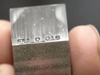
Fabrication of Single Crystal MgO Capsules
A method has been developed for machining MgO crystal blocks into forms for containing metallic and silicate liquids at temperatures up to 2,400 ºC, and pressures up to at least 320 kilobars. Possible custom shapes include tubes, rods, insulators, capsules, and guides. Key differences in this innovative...
Briefs: Manufacturing & Prototyping
Mars Aqueous Processing System
The goal of the Mars Aqueous Processing System (MAPS) is to establish a flexible process that generates multiple products that are useful for human habitation. Selectively extracting useful components into an aqueous solution, and then sequentially recovering individual constituents, can obtain a suite of refined or...
Briefs: Manufacturing & Prototyping
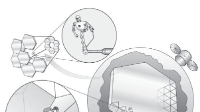
The NASA Human Space Flight program is interested in projects where humans, beyond low-Earth orbit (LEO), can make an important and unique contribution that cannot be reasonably...
Briefs: Manufacturing & Prototyping
High-precision mirrors for space applications are traditionally manufactured from one piece of material, such as lightweight glass “sandwich” or...
Briefs: Manufacturing & Prototyping
The sounding rocket experiment FIRE (Far-ultraviolet Imaging Rocket Experi ment) will improve the science community’s ability to image a spectral region hitherto unexplored...
Briefs: Manufacturing & Prototyping
Bulk metallic glasses (BMGs), a class of amorphous metals defined as having a thickness greater than 1 mm, are being broadly investigated by NASA for use in...
Briefs: Materials
High-Thermal-Conductivity Fabrics
Heat management with common textiles such as nylon and spandex is hindered by the poor thermal conductivity from the skin surface to cooling surfaces. This innovation showed marked improvement in thermal conductivity of the individual fibers and tubing, as well as components assembled from them.
Briefs: Manufacturing & Prototyping
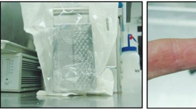
Projects that utilize large volumes of nonmetallic materials of planetary protection concern pose a challenge to their bioburden budget, as the most...
Briefs: Manufacturing & Prototyping
Demonstration of Minimally Machined Honeycomb Silicon Carbide Mirrors
Honeycomb silicon carbide composite mirrors are made from a carbon fiber preform that is molded into a honeycomb shape using a rigid mold. The carbon fiber honeycomb is densified by using polymer infiltration pyrolysis, or through a reaction with liquid silicon. A chemical vapor...
Briefs: Manufacturing & Prototyping
Heat Shield Employing Cured Thermal Protection Material Blocks Bonded in a Large-Cell Honeycomb Matrix
A document describes a new way to integrate thermal protection materials on external surfaces of vehicles that experience the severe heating environments of atmospheric entry from space. Cured blocks of thermal protection materials are bonded into...
Briefs: Manufacturing & Prototyping
Single-Layer, All-Metal Patch Antenna Element With Wide Bandwidth
It is known that the impedance at the center of a patch antenna element is a short circuit, implying that a wire or post can be connected from the patch to the groundplane at this point without impacting radiation performance. In principle, this central post can be used to support...
Briefs: Manufacturing & Prototyping
Scanning Laser Infrared Molecular Spectrometer (SLIMS)
This prototype innovation is a novel design that achieves very long, effective laser path lengths that are able to yield ppb (parts per billion) and sub-ppb measurements of trace gases. SLIMS can also accommodate multiple laser channels covering a wide range of wavelengths, resulting in...
Briefs: Manufacturing & Prototyping
Next-Generation Microshutter Arrays for Large-Format Imaging and Spectroscopy
A next-generation microshutter array, LArge Microshutter Array (LAMA), was developed as a multi-object field selector. LAMA consists of small-scaled microshutter arrays that can be combined to form large-scale microshutter array mosaics. Microshutter actuation is...
Briefs: Manufacturing & Prototyping
Techniques for Solution-Assisted Optical Contacting
A document discusses a “solution-assisted contacting” technique for optical contacting. An optic of surface flatness Lambda/20 was successfully contacted with one of “moderate” surface quality, or Lambda/4. Optics used were both ultra-low expansion (ULE) glass (Lambda/4 and Lambda/20) and...
Briefs: Manufacturing & Prototyping
Graphene Transparent Conductive Electrodes for Next- Generation Microshutter Arrays
Graphene is a single atomic layer of graphite. It is optically transparent and has high electron mobility, and thus has great potential to make transparent conductive electrodes. This invention contributes towards the development of graphene transparent conductive...
Briefs: Manufacturing & Prototyping
Fabrication of a Cryogenic Terahertz Emitter for Bolometer Focal Plane Calibrations
A fabrication process is reported for prototype emitters of THz radiation, which operate cryogenically, and should provide a fast, stable blackbody source suitable for characterization of THz devices. The fabrication has been demonstrated and, at the time of this...
Briefs: Manufacturing & Prototyping
Fabrication of an Absorber-Coupled MKID Detector
Absorber-coupled microwave kinetic inductance detector (MKID) arrays were developed for submillimeter and farinfrared astronomy. These sensors comprise arrays of lambda/2 stepped microwave impedance resonators patterned on a 1.5-mm-thick silicon membrane, which is optimized for optical coupling. The...
Briefs: Manufacturing & Prototyping
Processing of Nanosensors Using a Sacrificial Template Approach
A new microsensor fabrication approach has been demonstrated based upon the use of nanostructures as templates. The fundamental idea is that existing nanostructures, such as carbon nanotubes or biological structures, have a material structure that can be used advantageously in order to...
Briefs: Manufacturing & Prototyping
Fabrication of a Cryogenic Bias Filter for Ultrasensitive Focal Plane
A fabrication process has been developed for cryogenic in-line filtering for the bias and readout of ultrasensitive cryogenic bolometers for millimeter and submillimeter wavelengths. The design is a microstripline filter that cuts out, or strongly attenuates, frequencies (10–50...
Briefs: Manufacturing & Prototyping
Carbon Nanotube Bonding Strength Enhancement Using Metal “Wicking” Process
Carbon nanotubes grown from a surface typically have poor bonding strength at the interface. A process has been developed for adding a metal coat to the surface of carbon nanotubes (CNTs) through a “wicking” process, which could lead to an enhanced bonding strength...
Briefs: Manufacturing & Prototyping
Germanium Lift-Off Masks for Thin Metal Film Patterning
A technique has been developed for patterning thin metallic films that are, in turn, used to fabricate microelectronics circuitry and thin-film sensors. The technique uses germanium thin films as lift-off masks. This requires development of a technique to strip or undercut the germanium...
Briefs: Manufacturing & Prototyping
Multi-Layer Far- Infrared Component Technology
A method has been developed for fabricating high-reflectivity, multi-layer optical films for the terahertz wavelength region. A silicon mirror with 99.997-percent reflectivity at 70 μm wavelength requires an air gap of 17.50 μm, and a silicon thickness of 5.12 μm. This approach obtains pre-thinned...
Briefs: Manufacturing & Prototyping
The GeoLab glovebox was designed to enable the preliminary examination, by astronauts, of geological samples collected from the surface of another planetary body. The collected information would then...
Briefs: Manufacturing & Prototyping
Modified Process Reduces Porosity When Soldering in Reduced Gravity Environments
A modified process yields lower levels of internal porosity for solder joints produced in reduced-gravity environments. The process incorporates both alternative materials and a modified procedure. The process provides the necessary cleaning action to enable effective...
Briefs: Manufacturing & Prototyping
Self-Healing, Inflatable, Rigidizable Shelter
Any manned missions to extraterrestrial locations will require shelter structures for a variety of purposes ranging from habitat to biomass production. Such shelters need to be constructed in such a way as to minimize stowed volume and payload weight. The structures must also be very durable and have...
Briefs: Manufacturing & Prototyping
Improvements in Cold-Plate Fabrication
Five improvements are reported in cold-plate fabrication. This cold plate is part of a thermal control system designed to serve on space missions.
Briefs: Manufacturing & Prototyping
Fabrication of a Kilopixel Array of Superconducting Microcalorimeters With Microstripline Wiring
A document describes the fabrication of a two-dimensional microcalorimeter array that uses microstrip wiring and integrated heat sinking to enable use of high-performance pixel designs at kilo - pixel scales (32×32). Each pixel is the high-resolution...
Top Stories
Blog: Power
My Opinion: We Need More Power Soon — Is Nuclear the Answer?
Blog: AR/AI
Aerial Microrobots That Can Match a Bumblebee's Speed
News: Energy
Blog: Electronics & Computers
Turning Edible Fungi into Organic Memristors
Blog: Robotics, Automation & Control
Microscopic Swimming Machines that Can Sense, Respond to Surroundings
INSIDER: Sensors/Data Acquisition
Webcasts
 Upcoming Webinars: Energy
Hydrogen Engines Are Heating Up for Heavy Duty
 Upcoming Webinars: Transportation
Advantages of Smart Power Distribution Unit Design for Automotive...
 Upcoming Webinars: Automotive
Quiet, Please: NVH Improvement Opportunities in the Early Design...
 Upcoming Webinars: Test & Measurement
From Spreadsheets to Insights: Fast Data Analysis Without Complex...
 Upcoming Webinars: Power
Battery Abuse Testing: Pushing to Failure


