
Focal-plane arrays of semiconductor quantum-dot infrared photodetectors (QDIPs) are being developed as superior alternatives to prior infrared imagers, including imagers based on HgCdTe devices and, especially, those based on quantum-well infrared photodetectors (QWIPs). HgCdTe devices and arrays thereof are difficult to fabricate and operate, and they exhibit large nonunformities and high 1/f (where f signifies frequency) noise. QWIPs are easier to fabricate and operate, can be made nearly uniform, and exhibit lower 1/f noise, but they exhibit larger dark currents, and their quantization only along the growth direction prevents them from absorbing photons at normal incidence, thereby limiting their quantum efficiencies. Like QWIPs, QDIPs offer the advantages of greater ease of operation, greater uniformity, and lower 1/f noise, but without the disadvantages: QDIPs exhibit lower dark currents, and quantum efficiencies of QDIPs are greater because the threedimensional quantization of QDIPs is favorable to the absorption of photons at normal or oblique incidence. Moreover, QDIPs can be operated at higher temperatures (around 200 K) than are required for operation of QWIPs.
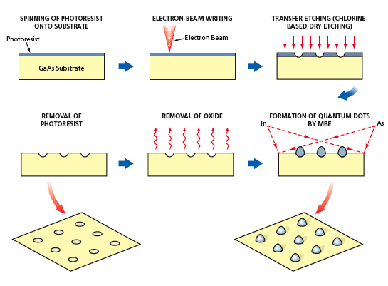
The exposed photoresist would be developed by either a high-contrast or a low-contrast method. In the high-contrast method, the spots would be etched in such a way as to form steep-wall holes all the way down to the substrate. The holes would be wider than the electron-beam spots — perhaps as wide as 15 to 20 nm, but may be sufficient to control the growth of the quantum dots. In the lowcontrast method, the resist would be etched in such a way as to form dimples, the shapes of which would mimic the electron-beam density profile. Then by use of a transfer etching process that etches the substrate faster than it etches the resist, either the pattern of holes or a pattern comprising the narrow, lowest portions of the dimples would be imparted to the substrate. Having been thus patterned, the substrate would be cleaned. The resulting holes or dimples in the substrate would serve as nucleation sites for the growth of quantum dots of controlled size in the following steps. The substrate would be cleaned, then placed in a molecular-beam-epitaxy (MBE) chamber, where native oxide would be thermally desorbed and the quantum dots would be grown.
This work was done by Sarath Gunapala, Daniel Wilson, Cory Hill, John Liu, Sumith Bandara, and David Ting of Caltech for NASA's Jet Propulsion Laboratory.NPO-41236.
This Brief includes a Technical Support Package (TSP).
Focal-Plane Arrays of Quantum-Dot Infrared Photodetectors
(reference NPO-41236) is currently available for download from the TSP library.
Don't have an account?
Overview
The document is a Technical Support Package from NASA's Jet Propulsion Laboratory (JPL) detailing advancements in Focal-Plane Arrays of Quantum-Dot Infrared Photodetectors (QDIPs), specifically identified by NTR Number 41236. It is part of NASA Tech Briefs, which aim to disseminate aerospace-related developments with broader technological, scientific, or commercial applications.
Quantum Dot Infrared Photodetectors represent a significant innovation in the field of imaging technology, particularly for space-based applications. These photodetectors utilize quantum dots—nanoscale semiconductor particles that have unique optical and electronic properties due to quantum mechanics. The document emphasizes the potential of QDIPs to enhance imaging capabilities in various aerospace missions, providing improved sensitivity and performance in detecting infrared light.
The Technical Support Package outlines the benefits of using QDIPs over traditional infrared detectors, including their ability to operate at higher temperatures and their tunable spectral response. This adaptability makes them suitable for a range of applications, from Earth observation to deep space exploration. The document also highlights the collaborative efforts under NASA's Commercial Technology Program, which aims to promote the commercialization of innovative technologies developed through government research.
For those interested in further information or collaboration, the document provides contact details for the Innovative Technology Assets Management office at JPL, encouraging engagement with the ongoing research and technology initiatives in this area.
Additionally, the document includes a notice regarding the proprietary nature of the information and the importance of complying with U.S. export regulations. It clarifies that the United States Government does not assume liability for the use of the information contained within the document, nor does it endorse any specific trade names or manufacturers mentioned.
In summary, this Technical Support Package serves as a comprehensive overview of the advancements in Quantum Dot Infrared Photodetector technology, highlighting its significance for future space-based imaging applications and inviting further exploration and collaboration in this innovative field.