
Dot-in-well (DWELL) quantum-dot infrared photodetectors (QDIPs) [DWELL-QDIPs] are subjects of research as potentially superior alternatives to prior QDIPs. Heretofore, there has not existed a reliable method for fabricating quantum dots (QDs) having precise, repeatable dimensions. This lack has constituted an obstacle to the development of uniform, high- performance, wavelength- tailorable QDIPs and of focal-plane arrays (FPAs) of such QDIPs. However, techniques for fabricating quantum-well infrared photodetectors (QWIPs) having multiple-quantum- well (MQW) structures are now well established. In the present research on DWELL-QDIPs, the arts of fabrication of QDs and QWIPs are combined with a view toward overcoming the deficiencies of prior QDIPs. The longer-term goal is to develop focal-plane arrays of radiation- hard, highly uniform arrays of QDIPs that would exhibit high performance at wavelengths from 8 to 15 μm when operated at temperatures between 150 and 200 K.
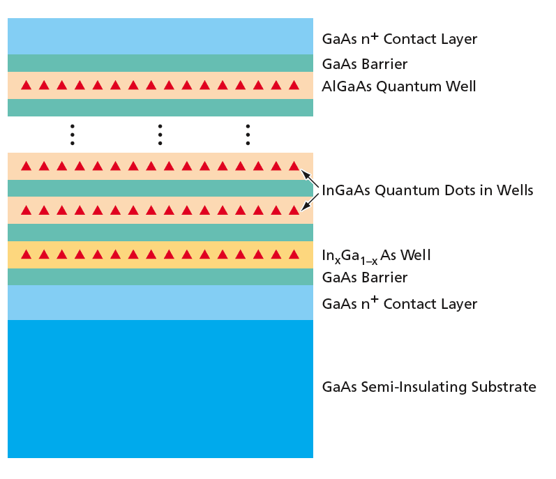
The approach being followed in the DWELL-QDIP research is to embed InGaAs QDs in GaAs/AlGaAs multiquantum- well (MQW) structures (see figure). This material system can accommodate a large number of QD layers without excessive lattice-mismatch strain and the associated degradation of photodetection properties. Hence, this material system is expected to enable achievement of greater densities of QDs and correspondingly greater quantum efficiencies. The host GaAs/AlGaAs MQW structures are highly compatible with mature fabrication processes that are now used routinely in making QWIP FPAs. The hybrid InGaAs-dot/GaAs/AlGaAs-well system also offers design advantages in that the effects of variability of dot size can be partly compensated by engineering quantum-well sizes, which can be controlled precisely.
Heretofore, a typical QDIP has exhibited high dark current attributable partly to a high-band-gap ohmic contact layer and partly to the fact that because of the low density of QDs, the QDs do not occupy all of the cross section presented to incident light and, hence, some of the current flowing in the device does not pass through the detector material. The undesired effect of the high-band-gap contact layer can be overcome by adding a high-band-gap barrier layer or placing an undoped spacer layer of GaAs, between about 500 and 600 Å thick between the quantum wells and the top contact layer. It has been previously demonstrated that such spacer layers can significantly reduce tunneling injection currents from contacts to quantum-well regions, thereby reducing dark currents.
Recently, it has been discovered that QDIPs exhibit strong QWIP-like intersubband absorption. The practical significance of this discovery is that it should be possible to increase the coupling of light into QDIPs, thereby increasing quantum efficiencies, by use of two-dimensional gratings.
This work was done by Sarath Gunapala, Sumith Bandara, David Ting, Cory Hill, John Liu, Jason Mumolo, and Yia Chung Chang of Caltech for NASA's Jet Propulsion Laboratory.
In accordance with Public Law 96-517, the contractor has elected to retain title to this invention. Inquiries concerning rights for its commercial use should be addressed to: Innovative Technology Assets
Management
JPL
Mail Stop 202-233
4800 Oak Grove Drive
Pasadena, CA 91109-8099
(818) 354-2240
E-mail:
Refer to NPO-42362, volume and number of this NASA Tech Briefs issue, and the page number.
This Brief includes a Technical Support Package (TSP).
Dot-in-Well Quantum-Dot Infrared Photodetectors
(reference NPO-42362) is currently available for download from the TSP library.
Don't have an account?
Overview
The document discusses advancements in Dot-in-Well Quantum-Dot Infrared Photodetectors (QDIPs), particularly focusing on the challenges and solutions associated with their development. It highlights the importance of improving quantum efficiency to enhance the competitiveness of QDIP-based focal plane array (FPA) technology. The primary issues identified include low quantum efficiency, high dark current, and inadequate surface coverage of quantum dots (QDOTs).
To address low quantum efficiency, the document suggests increasing the density of quantum dots and enhancing infrared absorption in the materials used. Current QDIPs primarily utilize InAs quantum dots on GaAs or within InGaAs/GaAs wells, but the limited number of quantum dot layers (typically five) restricts performance due to strain in the non-lattice matched materials. A promising alternative proposed is the use of InGaAs quantum dots embedded in GaAs/AlGaAs multi-quantum-well (MQW) structures, which can support a greater number of QD stacks without material degradation, thus improving quantum efficiency.
The document also addresses the issue of high dark current, which is attributed to the high band gap Ohmic contact layers and incomplete QDOT coverage. To mitigate this, the authors propose adding a thick (500-600 Å) undoped GaAs spacer layer between the quantum wells and the top contact layers, which has been shown to reduce tunneling injection current and lower dark current.
Additionally, the document notes that QDIP detectors exhibit strong intersubband absorption similar to quantum well infrared photodetectors (QWIPs). The implementation of a two-dimensional light coupling grating cavity is suggested as a method to significantly enhance the internal quantum efficiency of QDIPs.
The document emphasizes the JPL team's extensive experience in developing QWIPs and QDIPs, positioning them well to model, grow, and fabricate high-performance DWELL QDIPs for infrared FPAs used in remote sensing instruments. It concludes by noting that the highest detectivity achieved in QDIPs to date is 1×10^9 cmHz^1/2/W at 77 K, with reported responsivities of 50-60 mA/W, indicating ongoing challenges in achieving competitive performance compared to QWIPs. Overall, the document serves as a comprehensive overview of the current state and future directions of QDIP technology.