
The figure is a schematic diagram of a complementary metal oxide/semiconductor (CMOS) electronic circuit that functions as a NAND gate at a power-supply potential (Vdd) of 3.3 V and as NOR gate for Vdd = 1.8 V. In the intermediate Vdd range of 1.8 to 3.3 V, this circuit performs a function intermediate between NAND and NOR with degraded noise margin. Like the circuit of the immediately preceding article, this circuit serves as a demonstration of the evolutionary approach to design of polymorphic electronics — a technological discipline that emphasizes evolution of the design of a circuit to perform different analog and/or digital functions under different conditions. In this instance, the different conditions are different values of Vdd.
This demonstration is a step toward the development of a variety of logic gates, the functionalities of which can be changed by a single global signal — in this case, Vdd. The state-of-the-art logic circuits with which polymorphic logic circuits can be expected to compete are the configurable logic blocks (CLBs) of field-programmable gate arrays (FPGAs). The reconfiguration of a typical CLB involves multiplexing, switching, and downloading of thousands of bits from a lookup-table memory circuit. To configure in excess of thousands of CLBs in a larger FPGA may take even seconds; moreover, for satellite/spacecraft FPGA for which a new configuration is sent from Earth through a slow uplink communication, the time to reconfigure could be much longer. The main advantages of the type of polymorphism demonstrated here are the rapidity of the change in functionality and the simplicity of the circuitry needed to effect the change: Simply by changing Vdd, the functionalities of thousands of logic cells can be changed within nanoseconds, without multiplexing and without switches or lookup tables.
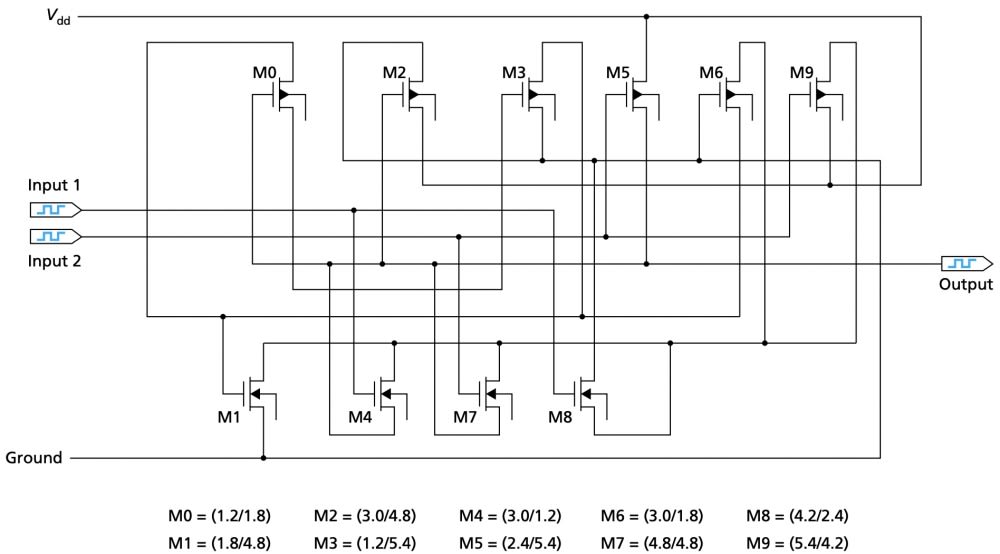
As in the case of the preceding article, the functionality of the present circuit has been tested by computational simulations. The simulations have tested the robustness of the circuit in the presence of input noise, for all possible sequences of positive and negative input-signal transitions, and under changes in parameters that include not only Vdd but, also temperature, switching speed, fan-out, and power dissipation. In addition, the circuit has been fabricated on a silicon chip and verified to function substantially as intended. This is the first circuit designed by artificial evolution to be so realized.
This work was done by Adrian Stoica and Ricardo Zebulum of Caltech for NASA’s Jet Propulsion Laboratory. For further information, access the Technical Support Package (TSP) free on-line at www.techbriefs.com/tsp under the Semiconductors & ICs category. NPO-30836
This Brief includes a Technical Support Package (TSP).
Multifunctional Logic Gate Controlled by Supply Voltage
(reference NPO-30836) is currently available for download from the TSP library.
Don't have an account?
Overview
The document titled "Multifunctional Logic Gate Controlled by Supply Voltage" presents a novel circuit technology developed by Ricardo S. Zebulum and Adrian Stoica, which allows a logic gate to change its functionality based on the power supply voltage (Vdd). This innovation is part of NASA's efforts to advance aerospace-related technologies with broader applications.
The circuit operates as a NAND gate when Vdd is set to 3.3V and as a NOR gate at 1.8V. For Vdd values between these two levels, the circuit exhibits an intermediate behavior with degraded noise margins. This adaptability is significant for applications requiring versatile logic operations without the need for multiple distinct circuits.
The document highlights that the circuit has been fabricated using HP 0.5μ technology and has undergone rigorous testing, confirming its predicted behavior from simulations. This achievement marks it as the first circuit synthesized through artificial evolution to be validated in silicon, showcasing the potential of evolutionary algorithms in circuit design.
Key performance metrics are discussed, including the circuit's switching time, which can be reduced significantly (to 20ns) for NAND functionality. The document also compares the total electric current of the multifunctional circuit with that of a conventional NOR gate, revealing that the peak current of the new circuit is an order of magnitude higher, indicating greater dynamic dissipation during transitions.
Figures included in the document illustrate the circuit schematic, layout, and response to varying Vdd levels, providing a visual representation of its functionality and performance characteristics. The authors emphasize the importance of optimizing transistor sizes to improve power consumption, which can enhance the circuit's efficiency.
Overall, this technical support package serves as a comprehensive overview of a groundbreaking logic gate technology that not only demonstrates the feasibility of multifunctional circuits but also opens avenues for further research and development in the field of electronics. The document is part of NASA's Commercial Technology Program, aimed at disseminating aerospace-related developments with potential commercial applications. For further inquiries, the document provides contact information for NASA's Scientific and Technical Information Program Office.