
Scanning filters based on surface plasmons would be used as the adjustable wavelength-selective (band-pass) devices in a class of proposed miniature spectrometers. These filters would occupy much less space and weigh much less than do the diffraction gratings and other wavelength-selective optics of conventional spectrometers; as a result, the proposed spectrometers would be correspondingly smaller and less massive.
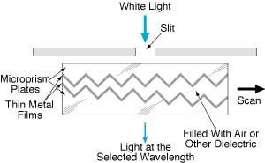
In a recently developed tunable band-pass filter [NASA Tech Briefs, Volume 22, No. 8 (August 1998), page 18a] based on surface plasmons, the pass wavelength band is adjusted by changing the airgap between two prisms. The filters in the proposed spectrometers would implement an alternative approach to tuning. A filter of this type would include two glass plates separated by a narrow gap filled with air or another dielectric with a low index of refraction. The facing surfaces of the plates would be grooved to form microprisms and coated with thin metal films. In a typical example, the dielectric would be air and the microprisms would be made of BK-7 (or equivalent) glass, formed for an angle of incidence of 41.5 °C, and coated with silver to a thickness of 40 nm.
The microprism plates would be tilted slightly to make the gap thickness vary from one edge to the other. The assembly of plates would be mounted on a scanning mechanism below a spectrometer slit, so that by use of the mechanism, the thickness of the gap illuminated through the slit could be varied. Inasmuch as the wavelength of peak transmission would depend on the thickness of the gap, scanning by use of the mechanism would thus result in variation of the pass wavelength band. In the example cited above, scanning from a gap 300 nm thick to a gap 5,000 nm thick would shift the wavelength of peak transmission from 400 to 1,600 nm.
This work was done by Yu Wang and Bedabrata Pain of Caltech for NASA's Jet Propulsion Laboratory. For further information, access the Technical Support Package (TSP) free on-line at www.techbriefs.com under the Physical Sciences category. NPO-20179
This Brief includes a Technical Support Package (TSP).
Scanning Surface-Plasmon Filters for Miniature Spectometers
(reference NPO20179) is currently available for download from the TSP library.
Don't have an account?
Overview
The document provides information about two significant engineering and technology expos scheduled for 1999: the New England Design & Manufacturing Expo in Boston and Technology 2009 in Miami Beach.
The New England Design & Manufacturing Expo will take place from September 20-22, 1999, at the Hynes Convention Center in Boston, Massachusetts. This event is designed to showcase the latest products and services that assist engineers in overcoming challenges related to design, prototyping, testing, and production. A notable feature of this expo is the CAD & Rapid Prototyping Pavilion, which highlights advancements in computer-aided design and rapid prototyping technologies. The expo is colocated with two other significant events: Photonics East, which is the only optics and photonics exhibition in the Northeast, and Electronic Imaging International, recognized as the East Coast’s premier annual imaging expo.
Following this, Technology 2009 will be held from November 1-3, 1999, at the Fontainebleau Hilton in Miami Beach, Florida. This event is touted as America’s premier showcase for new and next-generation technologies available for licensing and commercial development. It is the tenth annual “Engineering Innovation Show” and aims to connect innovators with potential partners and investors. Technology 2009 is also colocated with the Southeast Design & Manufacturing Expo, which targets the high-tech corridor of the Southeast, and the Small Business Tech Expo, which focuses on resources and technologies for launching new products and partnerships.
Both expos offer free admission to attendees, providing an excellent opportunity for networking, exploring cutting-edge technologies, and discovering new business ideas. The document encourages potential exhibitors and attendees to plan their visits and provides contact information for inquiries, including a website link and a contact person for exhibitors.
In summary, the document highlights two key events in the engineering and technology sectors, emphasizing their significance in fostering innovation, collaboration, and business development within the industry. It serves as a call to action for professionals to engage with the latest advancements and connect with peers in their fields.