
Circuits to generate analog or digital representations of the coordinates of the centers of mass of images would be added to imaging photodetector arrays of the active-pixel-sensor (APS) type, according to a proposal. "Centers of mass" as used here is something of a misnomer of historic origin; a more precise term would be "centers of illumination," or, the case of nonlinear or unequal photodetector responses, "centers of response." Regardless of which term one uses, the significance of the proposal is that it would enable APS units to locate and/or track still or moving images representing objects in various states of rest or motion.

For a given APS, the additional circuitry for computing the "center of mass" (COM) would be installed at the periphery of the pre-existing circuitry. The additional circuitry would thus not degrade the original optical properties or interfere with the original electronic functions of the APS. The APS could be operated in its normal image-readout mode, or optionally, it could be operated with the additional circuitry in a COM mode.
The objective in the COM mode is to generate numbers or analog signals representative of horizontal and vertical pixel coordinates of the center of illumination. In mathematical terms, what one seeks is the brightness-weighted (or response-to-brightness-weighted) average coordinates given by
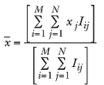
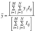
where x̄ and ȳ are the horizontal and vertical COM coordinates, respectively; xj is the horizontal coordinate of the jth column; yi is the vertical coordinate of the ith row; Iij is the level of illumination (or response to illumination) in the pixel in the ith row and jth column; and M and N are the numbers of rows and columns, respectively.
The COM operation could be implemented by use of analog peripheral circuitry like that shown in simplified form in the figure. Alternatively, the COM operation could be implemented by use of digital peripheral circuitry:
Taking one row at a time, the intensity-of-illumination signal from the pixel in each column would be sent to one of the input terminals of a multiplying digital-to-analog converter (MDAC). The column address or other number representative of the horizontal coordinate of the column would be sent to the other input terminal of the MDAC. The product outputs of all the MDACs for all the columns would be summed, then divided by the sum of intensity signals of the columns to obtain the horizontal COM coordinate of the row. Then x̄would be computed as an intensity-weighted average of the horizontal COM coordinates of all the rows, while ȳ= would be computed as an intensity-weighted average of the numerical addresses (or other numbers representative of the vertical coordinates) of the rows.
This work was done by Orly Yadid-Pecht, Brad Minch, Bedabrata Pain, and Eric Fossum of Caltech for NASA's Jet Propulsion Laboratory. In accordance with Public Law 96-517, the contractor has elected to retain title to this invention. Inquiries concerning rights for its commercial use should be addressed to
Technology Reporting Office
JPL
Mail Stop 122-116
4800 Oak Grove Drive
Pasadena, CA 91109
(818) 354-2240
Refer to NPO-20210
This Brief includes a Technical Support Package (TSP).
Augmented active-pixel sensors would compute centers of mass
(reference NPO20210) is currently available for download from the TSP library.
Don't have an account?
Overview
The document presents a proposal for integrating advanced functionality into Active Pixel Sensors (APS) through the development of a center-of-mass (COM) detection circuit. This innovation, attributed to inventors Orly Yadid-Pecht, Brad Minch, Bedabrata Pain, and Eric Fossum, aims to enhance the imaging capabilities of APS without degrading their performance. The proposed sensor can operate in two modes: a regular imaging mode and a COM mode, which allows for efficient tracking of moving objects by providing the center of mass address without the need to read the entire frame.
The significance of this technology lies in its potential applications across various fields, including NASA scientific endeavors, commercial, and consumer markets. The ability to track the center of mass is particularly valuable in scenarios such as star tracking, laser communications, and video conferencing, where high bandwidth tracking of moving objects is essential.
The document also discusses previous works related to COM detection in CMOS sensors, highlighting the limitations of earlier methods, such as those introduced by Steven Deweerth, which faced challenges in resolution and fill factor when extended to two dimensions. The proposed APS with integrated intelligence aims to overcome these limitations by maintaining a high fill factor while providing additional functionality.
Furthermore, the document clarifies the terminology used in the proposal, noting that "centers of mass" is somewhat of a misnomer. A more accurate term would be "centers of illumination" or "centers of response," especially in cases of nonlinear or unequal photodetector responses. This distinction emphasizes the sensor's capability to locate and track images representing objects in various states of motion or rest.
Overall, the proposal outlines a significant advancement in imaging technology, enabling APS to perform complex tasks such as tracking and locating objects efficiently. This innovation could lead to improved performance in a wide range of applications, making it a valuable contribution to the field of imaging sensors. The document serves as a technical support package for NASA, detailing the potential benefits and applications of the proposed APS technology.