Find the latest news and technical briefs on next-generation photonics technologies. Learn more about applications like biophotonics, silicon photonics, and green photonics.
Harvard research breakthrough could speed development of room‐temperature quantum computers…New generation of ultra‐lightweight, high‐res space cameras takes flight…NASA LiDAR advance gives...
Ongoing use of the laser has broadened the horizon of aerospace and defense capabilities by enabling the warfighter and through additive manufacturing processes that result in...
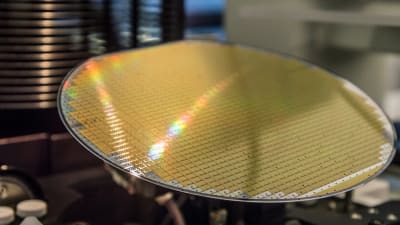
Miniaturization ranks as the driving force behind the semiconductor industry. The tremendous gains in computer performance since the 1950s are largely due to the fact that ever smaller...
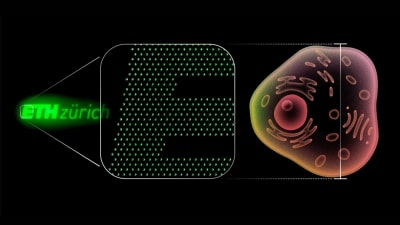
Optics researchers in the Harvard John A. Paulson School of Engineering and Applied Sciences created specially designed metasurfaces — flat devices etched with nanoscale light-manipulating patterns — to act as ultra-thin upgrades for quantum-optical chips and setups. Read on to learn more.
NASA's Glenn Research Center has developed a method of using entangled-photon pairs to produce highly secure mobile communications that require mere milliwatts of power. Read on to learn more.
Photonic processor enables ultrafast AI computations…how new polishing technique could revolutionize optical manufacturing…facial mapping technology is a leap forward in augmented reality. Read...
Researchers have been developing computers that deploy light, or photons, rather than electricity to power storage and calculations. These light-based computers...
NLM Photonics has confirmed that its patented silicon organic hybrid (SOH) photonic chips, featuring Selerion-HTX™ and JRD1, have successfully arrived at the International...
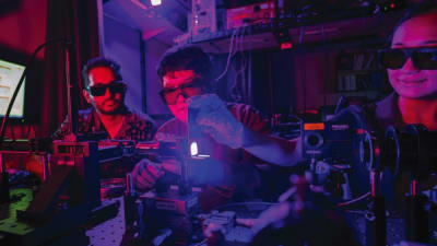
A few years ago, researchers in Michal Lipson’s Columbia Engineering lab noticed something remarkable. They were working on a project to design high-power chips that could...
Lasers vs. drones: military demonstrates new tech…high-‐flying uncrewed solar aircraft aces key test…the next frontier for autonomous UAVs. Read about these and other developments in this...
Critical advantages and challenges of using laser communications in space…the future of EMI protection for military aircraft…new "micro comb" chips promise to improve GPS accuracy. Read about these...
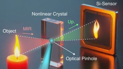
Researchers have used the centuries-old idea of pinhole imaging to create a high-performance mid-infrared imaging system without lenses. The new camera can capture extremely clear pictures over a large range of distances and in low light, making it useful for situations that are challenging for traditional cameras.
Known as FOSS (for fiber optic sensing system), NASA’s technology portfolio combines advanced sensors and innovative algorithms into a robust package that accurately and cost-effectively monitors a host of critical parameters in real time. Read on to learn more.
The Silicon Technology for Applications Relying on Light with Photonics Devices (STARLight) project brings together a consortium of leading industrial and...
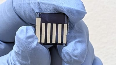
North Carolina State University engineers have built a tiny spectrometer that is orders of magnitude smaller than current technologies and can accurately measure wavelengths of light from ultraviolet to the near infrared.
See the new products, including Corning Incorporated's Corning® Gorilla® Glass Ceramic; Epoxy Technology's EPO-TEK®353NDP, a high-performance, humidity-resistant epoxy; Edmund Optics' off-the-shelf HOLO/OR Diffractive Diffusers and Beamsplitters; Teledyne Technologies subsidiary FLIR's advanced multispectral imaging solution; and much more.
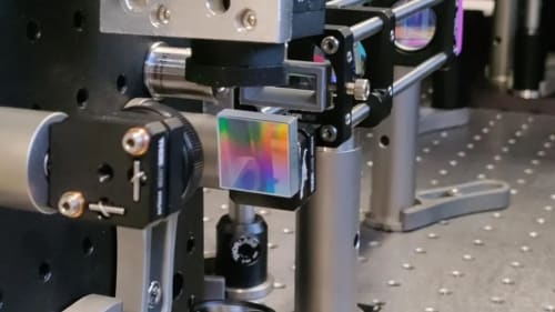
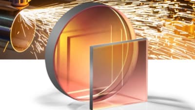
DPSS lasers are a critical enabling technology for meeting the precision materials processing demands of advanced packaging. Both nanosecond and USP lasers can achieve excellent results, but the right choice depends on specific requirements. Read on to learn more.
AI systems like ChatGPT are notorious for being power-hungry. To tackle this challenge, a team from the Centre for Optics, Photonics and Lasers has come up with an optical chip that can transfer massive amounts of data at ultra-high speed. As thin as a strand of hair, this technology offers unrivaled energy efficiency. Read on to learn more.
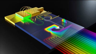
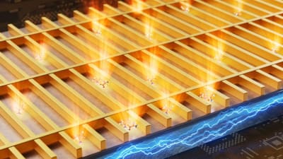
As fast as modern electronics have become, they could be much faster if their operations were based on light, rather than electricity. Fiber optic cables already transport information at the speed of light, but to do computations on that information without translating it back to electric signals will require a host of new optical components. Researchers have now developed such a device. Read on to learn more.
Engineers at the University of California San Diego have achieved a long-sought milestone in photonics: creating tiny optical devices that are both highly sensitive and durable — two qualities that have long been considered fundamentally incompatible. Read on to learn more.
Researchers have invented a new type of tunable semiconductor laser that combines the best attributes of today’s most advanced laser products, demonstrating smooth, reliable, wide-range wavelength tuning in a simple, chip-sized design. Read on to learn more about it.
For loading and unloading workpiece carriers containing wafers of different sizes in an automated process prior to PECVD coating, acp systems has developed a robotic solution aided by image processing for a leading manufacturer of space solar technology. Read on to learn more.
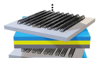
Researchers have developed an on-chip twisted moiré photonic crystal sensor that uses MEMS technology to control the gap and angle between the crystal layers in real time. The sensor can detect and collect detailed polarization and wavelength information simultaneously. Read on to learn more.
See the products of tomorrow, including a new tunable laser that uses a series of rings to smoothly emit many light wavelengths from a single chip; a smart capsule called PillTrek, which can measure pH, temperature, and a variety of different biomarkers; and more.
AI automates drone defense with high‐energy lasers…3D printing a game‐changer for ship and submarine part production…how TSN Ethernet will change the future of mil/aero...
With this groundbreaking discovery of time-dependent changes in networked nanodomains, developers are on the path to building adaptive networks for information storage and processing. Read on to learn more.
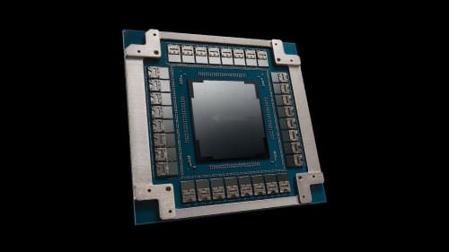
How advanced packaging is transforming mission‐critical electronics…a new era of high‐speed data transmission in defense…fully rugged PCs provide a decisive edge on the battlefield. Read about...